seveibar/f1c1990s-dev-board
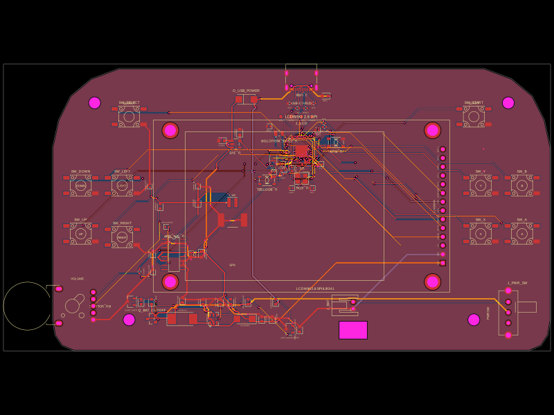
This code manages the entire PCB assembly process for a computer hardware module, including component placement, schematic integration, automated routing, copper pouring, and design rule checks, focused on a four-layer carrier board with integrated support components and connectors.
- Version
- 1.8.0
- License
- unset
- Stars
- 0
modules/f1c100s/docs/bulk-capacitors.md
> The dev board uses the modified **native** profile with all components on top. Other layout profiles retain their previously published two-sided layouts.

# Bulk capacitor selection

All seven rail reservoirs use 0805 land patterns on the top of the module. The three 10 µF TV/reference filter capacitors also use 0805 top-side footprints. Dedicated 100 nF processor decouplers remain on top with their direct pin branches. This is a single-sided component assembly.

| Role | Part | Nominal | Rating | Dielectric | Typical capacitance under DC bias |
|---|---|---|---|---|---|
| Six rail reservoirs and three TV/reference filters | GRM21BR61E106KA73L | 10 µF | 25 V | X5R | 7.21 µF at 3.3 V; 9.50 µF at 1.8 V |
| DRAM rail reservoir | GRM219R71E105KA88D | 1 µF | 25 V | X7R | 0.978 µF at 1.8 V |
| Six carrier regulator input/output reservoirs | GRM21BR71C475KE51L | 4.7 µF | 16 V | X7R | 3.31 µF at 5 V; 4.13 µF at 3.3 V |

The carrier regulator reservoirs remain on top and also use 0805 footprints. Capacitance values are unchanged from the original circuit. Larger packages do not guarantee the full nominal capacitance in service.

Typical values were interpolated from Murata's product-characteristics API on 2026-09-13 at 25 °C, with 1 Vrms test amplitude for the 10 µF and 1 µF parts and 0.5 Vrms for the 4.7 µF part. These are typical model results, not guaranteed minima; tolerance, temperature, aging and operating AC amplitude also matter. No PDN simulation or hardware measurements have been performed.

Sources: [10 µF part](https://pim.murata.com/en-us/pim/details/?partNum=GRM21BR61E106KA73%23), [1 µF part](https://pim.murata.com/en-us/pim/details/?partNum=GRM219R71E105KA88%23), [4.7 µF part](https://pim.murata.com/en-us/pim/details/?partNum=GRM21BR71C475KE51%23). Each product page exposes the C–DC-bias curves used here.

## Dev-board single-sided assembly revision

The native profile in this vendored copy places all bulk and reference capacitors on top. It replaces the earlier underside placement; capacitor values, 0805 sizes, voltage ratings and the dedicated 100 nF decouplers are retained. Stored routing is regenerated for the new placements.
Related Packages
 More from this authorseveibar/testpointsThis hardware consists of a small PCB with five test points arranged linearly, interconnected through a 1kΩ resistor and a 1000pF capacitor, forming a simple RC test configuration.
 Similar packageaura/diy-power-delivery-triggerThis hardware design implements a USB Type-C port with supporting power management and signal conditioning components, including a USB-C connector, a FUSB302 USB-C port controller, ESD protection diodes, a buck converter for 3.3V power regulation, an STM32 microcontroller for control and processing, an RGB LED indicator, push button, terminal block connections, and associated filtering and support components.
 Discover something newabse/gameboy-advanceThis code defines a collection of hardware components, including microcontrollers, sensors, display modules, power management ICs, and passive/passive components, each modeled as 3D symbols with specific footprints, pin configurations, and associated models for PCB and schematic design.