seveibar/f1c1990s-dev-board
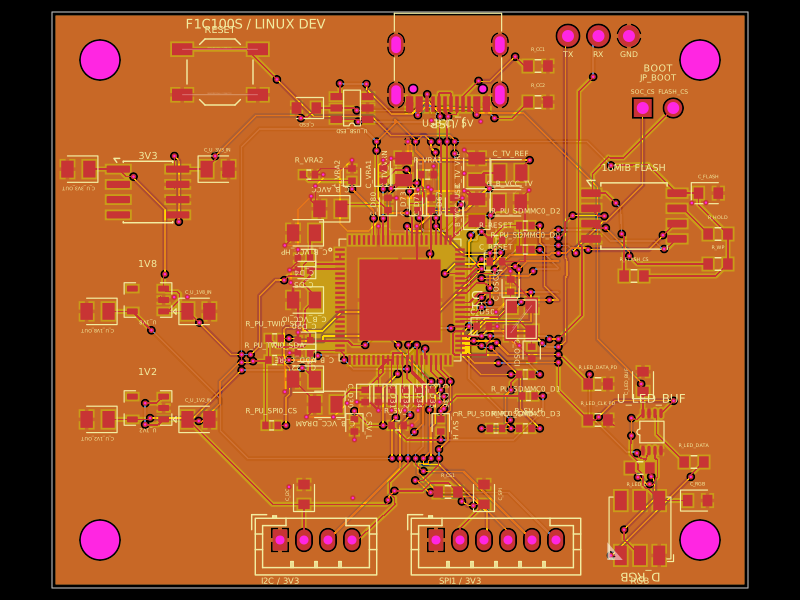
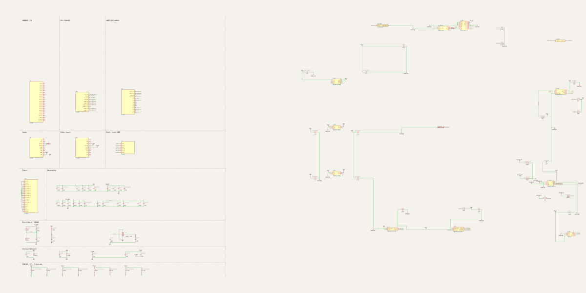
This code manages the entire PCB assembly process for a computer hardware module, including component placement, schematic integration, automated routing, copper pouring, and design rule checks, focused on a four-layer carrier board with integrated support components and connectors.
- Version
- 1.8.0
- License
- unset
- Stars
- 0
index.circuit.tsx
PCB
Schematic
import { SK9822_A } from "./imports/SK9822_A"
import { A_74AHCT2G125DC_125 } from "./imports/A_74AHCT2G125DC_125"
import { TYPE_C_31_M_12 } from "./imports/TYPE_C_31_M_12"
import { footprints } from "./footprints"
import { routingBoundaryRef } from "./routing-boundary"
import { F1C100SModule } from "./modules/f1c100s/src"

// 4-layer carrier; the imported module includes stored copper on all four layers.
const connect = (part: string, nets: string[]) => nets.map((net, i) =>
  net ? <trace key={`${part}-${i}`} from={`.${part} > .pin${i + 1}`} to={`net.${net}`} /> : null)
const cap = (name: string, value: string, net: string, x: number, y: number, rotation = 0, target?: string) => <>
  <capacitor name={name} capacitance={value} footprint={value === "4.7uF" ? "0805" : "0603"} maxVoltageRating={value === "4.7uF" ? 16 : undefined} manufacturerPartNumber={value === "4.7uF" ? "GRM21BR71C475KE51L" : undefined} pcbX={x} pcbY={y} pcbRotation={rotation} schX={x} schY={y} />
  <trace from={`.${name} > .pin1`} to={target ?? `net.${net}`} maxLength={target ? 5 : undefined} />
  <trace from={`.${name} > .pin2`} to="net.BOARD_GND" maxLength={1000} />
</>
const resistor = (name: string, value: string, a: string, b: string, x: number, y: number) => <>
  <resistor name={name} resistance={value} footprint="0603" pcbX={x} pcbY={y} schX={x} schY={y} />
  {connect(name, [a, b])}
</>
const jst = (name: string, nets: string[], x: number, y: number) => <>
  <chip name={name} manufacturerPartNumber={`B${nets.length}B-PH-K-S(LF)(SN)`}
    footprint={nets.length===6 ? footprints.jst6 : footprints.jst4}
    pinLabels={Object.fromEntries(nets.map((net, i) => [`pin${i + 1}`, net]))}
    pcbX={x} pcbY={y} schX={x} schY={y} />
  {connect(name, nets)}
</>
const ldoSo8 = (name: string, voltage: string, input: string, output: string, x: number, y: number) => <>
  <chip name={name} manufacturerPartNumber={`AP2112M-${voltage}TRG1`}
    footprint={footprints.so8}
    pinLabels={{pin1:"OUT",pin2:"NC2",pin3:"NC3",pin4:"NC4",pin5:"EN",pin6:"GND6",pin7:"GND7",pin8:"IN"}}
    pcbX={x} pcbY={y} schX={x} schY={y} />
  {connect(name, [output,"","","",input,"BOARD_GND","BOARD_GND",input])}
  {cap(`C_${name}_IN`, "4.7uF", input, x+5.8, y+1.905, 0, `.${name} > .pin8`)}
  {cap(`C_${name}_OUT`, "4.7uF", output, x-5.8, y+1.905, 180, `.${name} > .pin1`)}
</>

// AP2112K SOT-25: input 1, ground 2, enable 3, NC 4, output 5.
const ldoK = (name: string, voltage: string, output: string, x: number, y: number) => <>
  <chip name={name} manufacturerPartNumber={`AP2112K-${voltage}TRG1`}
    footprint="dfn6_missing(5)_p0.95mm_w3.5mm_pw0.5mm_pl0.9mm_pin1location(rightside,bottom)"
    pinLabels={{pin1:"IN",pin2:"GND",pin3:"EN",pin4:"NC",pin5:"OUT"}}
    pinAttributes={{pin2:{requiresGround:true},pin4:{doNotConnect:true}}}
    pcbX={x} pcbY={y} schX={x} schY={y} />
  {connect(name, ["V3V3","BOARD_GND","V3V3","",output])}
  {cap(`C_${name}_IN`, "4.7uF", "V3V3", x+4.2, y-0.95, 0, `.${name} > .pin1`)}
  {cap(`C_${name}_OUT`, "4.7uF", output, x-4.2, y-0.95, 180, `.${name} > .pin5`)}
</>

export default () => <board width={58} height={48} layers={4}
  minTraceWidth={0.12} minViaPadDiameter={0.45} minViaHoleDiameter={0.2}
  autorouter="auto-local" {...{ref:routingBoundaryRef}} schLayout={{layoutMode:"relative"}} schTraceAutoLabelEnabled schMaxTraceDistance={3}>
  <autoroutingphase autorouter="auto-local" minTraceToPadEdgeClearance={0.13} minPadEdgeToPadEdgeClearance={0.13} minViaEdgeToPadEdgeClearance={0.13} />
  <keepout shape="rect" width={25.6} height={25.6} pcbX={0} pcbY={0}
    layers={["top","inner1","inner2","bottom"]} excludeRefs={[".SOC *"]} />
  {/* Protect the stored east-edge module trace from carrier routing. */}
  <keepout shape="rect" width={0.8} height={1.1} pcbX={13.3} pcbY={2.65}
    layers={["top","inner1","inner2","bottom"]} excludeRefs={[".SOC *"]} />
  <net name="BOARD_GND" isGroundNet />
  <net name="V5_IN" nominalTraceWidth={0.12} />
  <net name="V3V3" nominalTraceWidth={0.12} />
  <net name="V1V8" nominalTraceWidth={0.12} />
  <net name="V1V2" nominalTraceWidth={0.12} />
  <F1C100SModule name="SOC" layoutProfile="native" pcbX={0} pcbY={0} schX={-70} schY={0}
    connections={{
      GND:"net.BOARD_GND", VDD_CORE:"net.V1V2", VCC_DRAM:"net.V1V8",
      VCC_IO:"net.V3V3", VCC_USB:"net.V3V3", AVCC:"net.V3V3",
      VCC_HP:"net.V3V3", VCC_TV:"net.V3V3",
      SPI0_CLK:"net.FLASH_CLK", SPI0_CS:"net.SOC_FLASH_CS",
      SPI0_MOSI:"net.FLASH_MOSI", SPI0_MISO:"net.FLASH_MISO",
      PE7:"net.SPI1_CS", PE8:"net.SPI1_MOSI", PE9:"net.SPI1_CLK", PE10:"net.SPI1_MISO",
      TWI0_SDA:"net.I2C_SDA", TWI0_SCL:"net.I2C_SCL",
      UART0_TX:"net.UART_TX", UART0_RX:"net.UART_RX",
      USB_DM:"net.USB_N", USB_DP:"net.USB_P", RESET:"net.RESET_N",
      PE2:"net.LED_DATA_3V3", PE3:"net.LED_CLK_3V3",
    }} />

  {/* USB 2.0 device/sink: separate Rd resistors for both plug orientations. */}
  <TYPE_C_31_M_12 name="J_USB" pcbX={4} pcbY={18.5} pcbRotation={180}
    schX={4} schY={20} />
  {connect("J_USB", ["BOARD_GND","BOARD_GND","BOARD_GND","BOARD_GND","","USB_CC1","USB_N","USB_P","","","","USB_CC2","BOARD_GND","BOARD_GND","V5_IN","V5_IN"])}
  <trace name="USB_DM_REVERSIBLE" from=".J_USB > .pin7" to=".J_USB > .pin9" maxLength={4} pcbPath={[".J_USB > .pin7",{x:-0.750062,y:3.1},{x:0.249936,y:3.1},".J_USB > .pin9"]} />
  <trace name="USB_DP_REVERSIBLE" from=".J_USB > .pin8" to=".J_USB > .pin10" maxLength={4} pcbPath={[".J_USB > .pin8",{x:-0.249936,y:1.25},{x:0.750062,y:1.25},".J_USB > .pin10"]} />
  {resistor("R_CC1", "5.1k", "USB_CC1", "BOARD_GND", 11.5, 19.5)}
  {resistor("R_CC2", "5.1k", "USB_CC2", "BOARD_GND", 11.5, 16.5)}
  {/* Bare 2.54 mm pitch solder/debug holes, not fitted assembly parts. */}
  {(["TX","RX","GND"] as const).map((signal,i)=><group key={signal} pcbX={0} pcbY={0}>
    <testpoint name={`TP_UART_${signal}`} pcbX={14+i*2.54} pcbY={22}
      footprint={<footprint><platedhole portHints={["pin1"]} holeDiameter={1} outerDiameter={1.8} shape="circle" /></footprint>} />
    <trace from={`.TP_UART_${signal} > .pin1`} to={`net.${signal==="GND"?"BOARD_GND":`UART_${signal}`}`} />
    <silkscreentext text={signal} pcbX={14+i*2.54} pcbY={20.5} fontSize={0.65} />
  </group>)}
  {jst("J_SPI", ["BOARD_GND","V3V3","SPI1_CLK","SPI1_MOSI","SPI1_MISO","SPI1_CS"], 3, -20)}
  {jst("J_I2C", ["BOARD_GND","V3V3","I2C_SDA","I2C_SCL"], -10, -20)}
  {resistor("R_CS1", "10k", "SPI1_CS", "V3V3", 4, -16)}
  {/* TWI0 already has 4.7 kΩ pull-ups inside the module. */}
  {cap("C_SPI", "100nF", "V3V3", 7, -16.2, 90)}
  {cap("C_I2C", "100nF", "V3V3", -8, -16.2, 90)}

  {/* AP2112 SO-8 version: output 1, EN 5, GND 6/7, input 8. */}
  {ldoSo8("U_3V3", "3.3", "V5_IN", "V3V3", -21, 9)}
  {ldoK("U_1V8", "1.8", "V1V8", -21, 0)}
  {ldoK("U_1V2", "1.2", "V1V2", -21, -9)}

  {/* 16 MiB SPI NOR for SPL / U-Boot / compact Linux + rootfs. */}
  <chip name="U_FLASH" manufacturerPartNumber="W25Q128JVSIQ"
    footprint={footprints.flash}
    pinLabels={{pin1:"CS_N",pin2:"DO",pin3:"WP_N",pin4:"BOARD_GND",pin5:"DI",pin6:"CLK",pin7:"HOLD_N",pin8:"VCC"}}
    pcbX={19.5} pcbY={7} schX={23} schY={7} />
  {connect("U_FLASH", ["FLASH_CS","FLASH_MISO","FLASH_WP","BOARD_GND","FLASH_MOSI","FLASH_CLK","FLASH_HOLD","V3V3"])}
  {cap("C_FLASH", "100nF", "V3V3", 25.7, 8.905, 0, ".U_FLASH > .pin8")}
  {resistor("R_WP", "10k", "FLASH_WP", "V3V3", 26.5, 3)}
  {resistor("R_HOLD", "10k", "FLASH_HOLD", "V3V3", 26.5, 5.5)}
  {resistor("R_FLASH_CS", "10k", "FLASH_CS", "V3V3", 19.5, 2)}
  <chip name="JP_BOOT" footprint="pinrow2_p2.54" pinLabels={{pin1:"SOC_CS",pin2:"FLASH_CS"}} pcbX={21.5} pcbY={16} schX={23} schY={17} />
  {connect("JP_BOOT", ["SOC_FLASH_CS","FLASH_CS"])}

  <chip name="SW_RESET" footprint={footprints.reset}
    manufacturerPartNumber="TL3342F160QG" pinLabels={{pin1:"RESET",pin2:"BOARD_GND"}} pcbX={-15} pcbY={19} schX={-12} schY={20} />
  {connect("SW_RESET", ["RESET_N","BOARD_GND"])}
  {/* USBLC6-2SC6: shunt ESD protection; duplicate IO pads are internally common. */}
  <chip name="U_USB_ESD" manufacturerPartNumber="USBLC6-2SC6" footprint="sot23_6"
    pinLabels={{pin1:"DM1",pin2:"BOARD_GND",pin3:"DP1",pin4:"DP2",pin5:"VBUS",pin6:"DM2"}}
    pcbX={-4} pcbY={16} pcbRotation={180} schX={0} schY={19.5} />
  {connect("U_USB_ESD", ["USB_N","BOARD_GND","USB_P","USB_P","V5_IN","USB_N"])}
  {cap("C_ESD", "100nF", "V5_IN", -7.8, 16, 180, ".U_USB_ESD > .pin5")}

  {/* Clocked RGB LED: PE2=data, PE3=clock. AHCT accepts 3.3 V logic at 5 V. */}
  <SK9822_A name="D_RGB" pcbX={20} pcbY={-19} pcbRotation={180} schX={25} schY={-21} />
  {connect("D_RGB", ["BOARD_GND","V5_IN","","","LED_DATA","LED_CLK"])}
  <A_74AHCT2G125DC_125 name="U_LED_BUF" pcbX={21} pcbY={-11} schX={21} schY={-11} />
  {connect("U_LED_BUF", ["BOARD_GND","LED_DATA_3V3","LED_CLK_5V","BOARD_GND","LED_CLK_3V3","LED_DATA_5V","BOARD_GND","V5_IN"])}
  {resistor("R_LED_DATA", "470", "LED_DATA_5V", "LED_DATA", 24.5, -13.5)}
  {resistor("R_LED_CLK", "470", "LED_CLK_5V", "LED_CLK", 20, -14)}
  {resistor("R_LED_DATA_PD", "100k", "LED_DATA_3V3", "BOARD_GND", 16.5, -7)}
  {resistor("R_LED_CLK_PD", "100k", "LED_CLK_3V3", "BOARD_GND", 16.5, -10)}
  {cap("C_RGB", "100nF", "V5_IN", 24.8, -16.712476, 0, ".D_RGB > .pin2")}
  {cap("C_LED_BUF", "100nF", "V5_IN", 20.249938, -6.8, 90, ".U_LED_BUF > .pin8")}

  {([-25,25] as const).flatMap(x => ([-20,20] as const).map(y =>
    <hole {...{key:`${x}-${y}`}} name={`H_${x}_${y}`} diameter={3.2} pcbX={x} pcbY={y} />))}
  <silkscreentext text="RESET" pcbX={-15} pcbY={22.5} fontSize={0.8} />
  <silkscreentext text="3V3" pcbX={-21} pcbY={12} fontSize={0.8} />
  <silkscreentext text="1V8" pcbX={-21} pcbY={3} fontSize={0.8} />
  <silkscreentext text="1V2" pcbX={-21} pcbY={-6} fontSize={0.8} />
  <silkscreentext text="16MiB FLASH" pcbX={19.5} pcbY={11} fontSize={0.8} />
  <silkscreentext text="F1C100S / LINUX DEV" pcbX={-12} pcbY={23} fontSize={1.1} />
  <silkscreentext text="USB-C / 5V" pcbX={4} pcbY={14.7} fontSize={0.8} />
  <silkscreentext text="I2C / 3V3" pcbX={-10} pcbY={-23.4} fontSize={0.7} />
  <silkscreentext text="SPI1 / 3V3" pcbX={5} pcbY={-23.4} fontSize={0.7} />
  <silkscreentext text="BOOT" pcbX={21.5} pcbY={19.3} fontSize={0.8} />
  <silkscreentext text="RGB" pcbX={20} pcbY={-23.4} fontSize={0.7} />
  {(["top","inner1","inner2","bottom"] as const).map(layer =>
    <copperpour {...{key:layer}} layer={layer} connectsTo="net.BOARD_GND" clearance={0.15}
      boardEdgeMargin={0.3} useThermalReliefs coveredWithSolderMask />)}
</board>
Related Packages
 More from this authorseveibar/testpointsThis hardware consists of a small PCB with five test points arranged linearly, interconnected through a 1kΩ resistor and a 1000pF capacitor, forming a simple RC test configuration.
 Similar packageaura/diy-power-delivery-triggerThis hardware design implements a USB Type-C port with supporting power management and signal conditioning components, including a USB-C connector, a FUSB302 USB-C port controller, ESD protection diodes, a buck converter for 3.3V power regulation, an STM32 microcontroller for control and processing, an RGB LED indicator, push button, terminal block connections, and associated filtering and support components.
 Discover something newabse/gameboy-advanceThis code defines a collection of hardware components, including microcontrollers, sensors, display modules, power management ICs, and passive/passive components, each modeled as 3D symbols with specific footprints, pin configurations, and associated models for PCB and schematic design.