seveibar/f1c1990s-dev-board
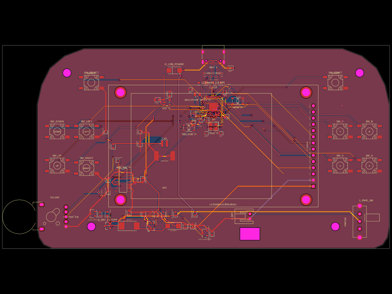
This code manages the entire PCB assembly process for a computer hardware module, including component placement, schematic integration, automated routing, copper pouring, and design rule checks, focused on a four-layer carrier board with integrated support components and connectors.
- Version
- 1.8.0
- License
- unset
- Stars
- 0
imports/SK9822_A.tsx
import type { ChipProps } from "@tscircuit/props"

const pinLabels = {
  pin1: ["GND"],
  pin2: ["VCC"],
  pin3: ["CKO"],
  pin4: ["SDO"],
  pin5: ["SDI"],
  pin6: ["CKI"]
} as const

const pinAttributes = {
  pin1: {requiresGround: true},
  pin2: {requiresPower: true}
} as const

export const SK9822_A = (props: ChipProps<typeof pinLabels>) => {
  return (
    <chip
      pinLabels={pinLabels}
      pinAttributes={pinAttributes}
      supplierPartNumbers={{
  "jlcpcb": [
    "C5378730"
  ]
}}
      manufacturerPartNumber="SK9822-A"
      footprint={<footprint>
        <smtpad portHints={["pin4"]} pcbX="1.599946mm" pcbY="-2.287524mm" width="0.999998mm" height="1.6249904mm" shape="rect" />
<smtpad portHints={["pin3"]} pcbX="0mm" pcbY="-2.287524mm" width="0.999998mm" height="1.6249904mm" shape="rect" />
<smtpad portHints={["pin2"]} pcbX="-1.599946mm" pcbY="-2.287524mm" width="0.999998mm" height="1.6249904mm" shape="rect" />
<smtpad portHints={["pin5"]} pcbX="1.599946mm" pcbY="2.287524mm" width="0.999998mm" height="1.6249904mm" shape="rect" />
<smtpad portHints={["pin6"]} pcbX="0mm" pcbY="2.287524mm" width="0.999998mm" height="1.6249904mm" shape="rect" />
<smtpad portHints={["pin1"]} pcbX="-1.599946mm" pcbY="2.287524mm" width="0.999998mm" height="1.6249904mm" shape="rect" />
<silkscreenpath route={[{"x":-2.7939999999999827,"y":2.227707000000123},{"x":-2.7939999999999827,"y":2.717774600000098},{"x":-2.7939999999999827,"y":2.7940000000000964},{"x":-2.29400099999998,"y":2.7940000000000964}]} />
<silkscreenpath route={[{"x":-2.238527399999839,"y":-2.5761695999999574},{"x":-2.5761695999999574,"y":-2.5761695999999574},{"x":-2.5761695999999574,"y":2.5761949999999842},{"x":-2.238527399999839,"y":2.5761949999999842}]} />
<silkscreenpath route={[{"x":2.2384766000000127,"y":-2.5761695999999574},{"x":2.5761949999999842,"y":-2.5761695999999574},{"x":2.5761949999999842,"y":2.5761949999999842},{"x":2.2384766000000127,"y":2.5761949999999842}]} />
<silkscreentext text="{NAME}" pcbX="0.000254mm" pcbY="4.100324mm" anchorAlignment="center" fontSize="1mm" />
<fabricationnotepath route={[{"x":2.603474600000027,"y":1.5240254000000277},{"x":2.603474600000027,"y":2.5400253999999904},{"x":1.7144746000000168,"y":2.5400253999999904},{"x":2.603474600000027,"y":1.5240254000000277}]} strokeWidth="0.254mm" />
<courtyardoutline outline={[{"x":-3.043745999999828,"y":3.350323999999887},{"x":3.0442540000000236,"y":3.350323999999887},{"x":3.0442540000000236,"y":-3.347276000000079},{"x":-3.043745999999828,"y":-3.347276000000079},{"x":-3.043745999999828,"y":3.350323999999887}]} />
      </footprint>}
      cadModel={{
        objUrl: "https://modelcdn.tscircuit.com/easyeda_models/assets/C5378730.obj?uuid=bc532e8be81044cd8717cb5acdb4d158",
        stepUrl: "https://modelcdn.tscircuit.com/easyeda_models/assets/C5378730.step?uuid=bc532e8be81044cd8717cb5acdb4d158",
        pcbRotationOffset: 90,
        modelOriginPosition: { x: -0.000012699999956566899, y: -0.004999999999999893, z: -0.82 },
      }}
      {...props}
    />
  )
}
Related Packages
 More from this authorseveibar/testpointsThis hardware consists of a small PCB with five test points arranged linearly, interconnected through a 1kΩ resistor and a 1000pF capacitor, forming a simple RC test configuration.
 Similar packageaura/diy-power-delivery-triggerThis hardware design implements a USB Type-C port with supporting power management and signal conditioning components, including a USB-C connector, a FUSB302 USB-C port controller, ESD protection diodes, a buck converter for 3.3V power regulation, an STM32 microcontroller for control and processing, an RGB LED indicator, push button, terminal block connections, and associated filtering and support components.
 Discover something newabse/gameboy-advanceThis code defines a collection of hardware components, including microcontrollers, sensors, display modules, power management ICs, and passive/passive components, each modeled as 3D symbols with specific footprints, pin configurations, and associated models for PCB and schematic design.