pixalynx/esp32-usb-ducky
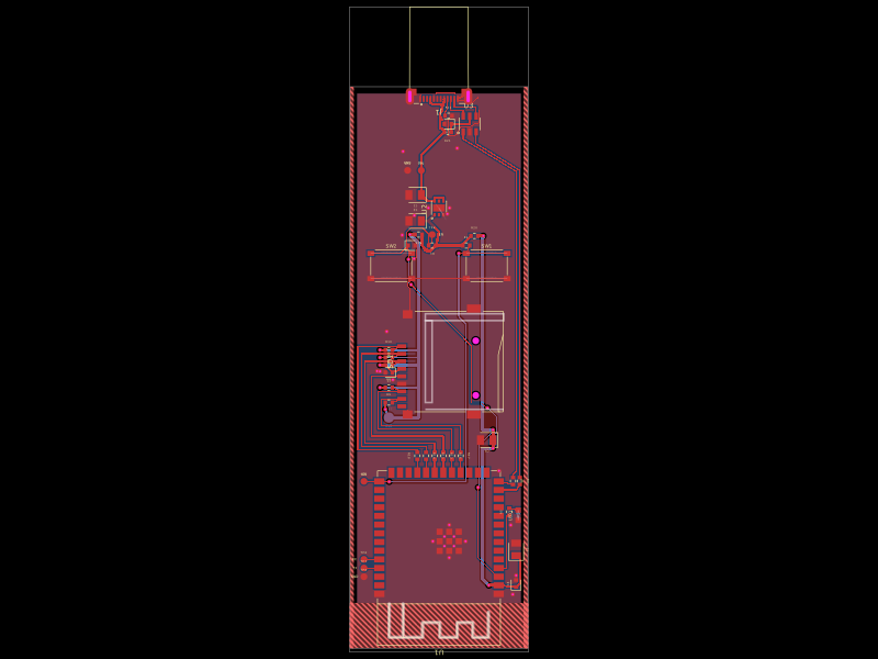
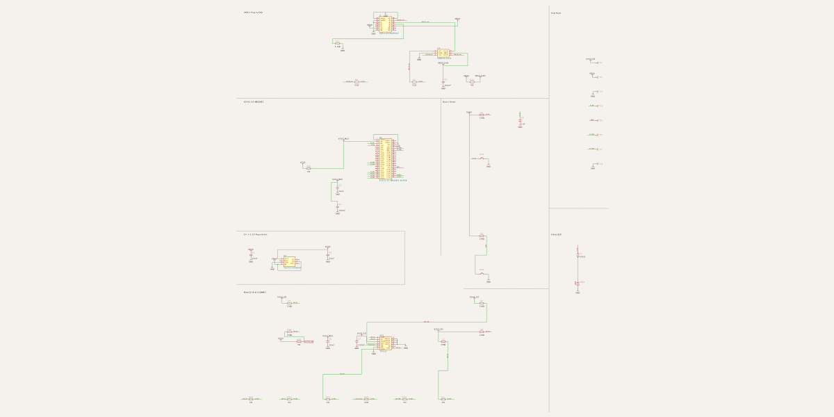
This code defines digital and analog ICs, connectors, and components with specified pinouts, footprints, and 3D models for PCB rendering, including voltage regulators, USB connectors, microSD sockets, and push-button switches.
- Version
- 1.2.6
- License
- unset
- Stars
- 0
index.circuit.tsx
PCB
Schematic
import { Fragment } from "react"
import { ESP32_S3_WROOM_1_N16R8 } from "./imports/ESP32_S3_WROOM_1_N16R8"
import { TLV75733PDRVR } from "./imports/TLV75733PDRVR"
import { USBLC6_2SC6 } from "./imports/USBLC6_2SC6"
import { TF_01A } from "./imports/TF_01A"
import { TS_1187A_B_A_B } from "./imports/TS_1187A_B_A_B"
import { U261_121N_4BS2S } from "./imports/U261_121N_4BS2S"
import { XL_1608UBC_04 } from "./imports/XL_1608UBC_04"

// Schematic sections on a compact grid.
const SEC = {
  Usb: { x: 0, y: 16 },
  Mcu: { x: 0, y: 2 },
  BootReset: { x: 10, y: 2 },
  Power: { x: -10, y: -8 },
  Indicator: { x: 20, y: -8 },
  MicroSd: { x: 0, y: -20 },
  Test: { x: 22, y: 8 },
}

// Board outline is a plain 26 x 82.25mm stick. The USB-C male plug (J1) is a
// board-edge part: its SMD contacts and shell pegs sit on the PCB and the
// 11.25mm plug body overhangs the TOP edge to insert straight into a host.
// XKB's recommended PCB layout puts the board edge at the outer end of the
// shell-peg pads, which is also where JLCPCB's EasyEDA footprint starts its
// board cutout: y = 33.25 here, 0.22mm past the slot copper (JLCPCB's routed
// edge minimum is 0.2mm). v1.2.5 ran the board 2.25mm further under the plug.
// The ESP32 module lives at the BOTTOM with its printed antenna right at the
// bottom edge, as far from the USB metal as the board allows.
//   top edge (USB-C plug)   y = +33.25
//   bottom edge (antenna)   y = -49
const EDGE_TOP = 33.25
const EDGE_BOTTOM = -49
const BOARD_OUTLINE = [
  { x: -13, y: EDGE_BOTTOM },
  { x: 13, y: EDGE_BOTTOM },
  { x: 13, y: EDGE_TOP },
  { x: -13, y: EDGE_TOP },
]
const EDGE_FENCE = { pcbY: (EDGE_TOP + EDGE_BOTTOM) / 2, height: EDGE_TOP - EDGE_BOTTOM }
// The board's centre is pcbY + outlineOffsetY and every outline point is
// shifted by the same offset, so the outline is written relative to its own
// centre. That keeps the edges where they are while the board box DRC and
// the placement checker derive (centre +/- height/2) matches the outline.
const BOARD_CENTER_Y = (EDGE_TOP + EDGE_BOTTOM) / 2
const BOARD_OUTLINE_REL = BOARD_OUTLINE.map((p) => ({ x: p.x, y: p.y - BOARD_CENTER_Y }))

// U1 is placed antenna-down (pcbRotation=180) at the bottom. Its printed
// antenna (the module's own meander) sits flush at the bottom board edge
// with no copper around or under it — the proper spot for RF, well clear of
// the USB shell up top. The keepout spans the FULL board width (26mm) so the
// GND pours can't fill the strips beside the antenna down to the board edge
// (Espressif's module guidelines want the sides of the antenna clear, not just
// the area under it).
const ANTENNA_KEEPOUT = { pcbX: 0, pcbY: -45.65, width: 26.2, height: 6.6 }

// JLCPCB part for every passive, pinned so the BOM cannot drift when the
// parts engine picks differently in a later tscircuit release.
const JLC = {
  R_0_0402: { jlcpcb: ["C17168"] },
  R_22_0402: { jlcpcb: ["C25092"] },
  R_330_0402: { jlcpcb: ["C25104"] },
  R_5K1_0402: { jlcpcb: ["C25905"] },
  R_10K_0402: { jlcpcb: ["C25744"] },
  C_100N_0402: { jlcpcb: ["C1525"] },
  C_1U_0402: { jlcpcb: ["C52923"] },
  C_10U_0805: { jlcpcb: ["C15850"] },
  C_22U_0805: { jlcpcb: ["C45783"] },
}

type Pt = { x: number; y: number }
type Rot = 0 | 90 | 180 | 270
type Layer = "top" | "bottom"

// A <trace pcbPath> point is an offset from the from-pad component's pcbX/pcbY
// (not its land-pattern centre), rotated with that component. frame()
// converts board coordinates. Only the few non-critical links left on pcbPath
// use it; the router may still adjust those.
const frame =
  (c: Pt, rot: Rot = 0) =>
  (p: Pt): Pt => {
    const dx = p.x - c.x
    const dy = p.y - c.y
    if (rot === 90) return { x: dy, y: -dx }
    if (rot === 180) return { x: -dx, y: -dy }
    if (rot === 270) return { x: -dy, y: dx }
    return { x: dx, y: dy }
  }

// Board position of pin1/pin2 of a 2-pad passive (0402 offset 0.51mm, 0805
// 0.9125mm) placed at c with the given pcbRotation.
const pin = (c: Pt, rot: Rot, offset: number, which: 1 | 2): Pt => {
  const d = which === 1 ? -offset : offset
  const f = rot === 0 ? { x: d, y: 0 } : rot === 90 ? { x: 0, y: d } : rot === 180 ? { x: -d, y: 0 } : { x: 0, y: -d }
  return { x: c.x + f.x, y: c.y + f.y }
}

// ------------------------------------------------------------------------
// LOCKED ROUTES. tscircuit 0.0.2561's autorouter treats plain pcbPath traces
// as suggestions: it rewrote a third of them and routed other nets through
// them. Every critical connection is therefore a SAVED route in routing
// phase 0 (<autoroutingphase pcbTracePaths>): core hands the saved copper to
// the router as fixed obstacles, so it is never moved and nothing is routed
// through it. Rules: a saved route is written in board mm, must start and end
// exactly on PCB port positions, and phase 0 must cover every pad of every
// connection assigned to it (routingPhaseIndex={0} on those traces). Pads of
// a multi-pad net are chained: each route starts at a pad not yet joined.
// ------------------------------------------------------------------------
type SavedPoint =
  | { route_type: "wire"; x: number; y: number; width: number; layer: Layer }
  | { route_type: "via"; x: number; y: number; from_layer: Layer; to_layer: Layer }
// "via" changes layer at the previous point.
const savedRoute = (width: number, pts: (Pt | "via")[], startLayer: Layer = "top"): SavedPoint[] => {
  let layer = startLayer
  let last = pts[0] as Pt
  const out: SavedPoint[] = []
  for (const p of pts) {
    if (p === "via") {
      const to: Layer = layer === "top" ? "bottom" : "top"
      out.push({ route_type: "via", x: last.x, y: last.y, from_layer: layer, to_layer: to })
      layer = to
      continue
    }
    out.push({ route_type: "wire", x: p.x, y: p.y, width, layer })
    last = p
  }
  return out
}
const mid = (a: Pt, b: Pt): Pt => ({ x: (a.x + b.x) / 2, y: (a.y + b.y) / 2 })

// Exact PCB port positions of imported footprints (from circuit.json).
const PORT = {
  SD1_DAT2: { x: -5.45108765, y: -4.759986699999999 },
  SD1_CS: { x: -5.45108765, y: -5.8600353 },
  SD1_MOSI: { x: -5.45108765, y: -6.9600839 },
  SD1_VDD: { x: -5.45108765, y: -8.0601325 },
  SD1_SCK: { x: -5.45108765, y: -9.1599525 },
  SD1_MISO: { x: -5.45108765, y: -11.360049700000001 },
  SD1_DAT1: { x: -5.45108765, y: -12.459869699999999 },
  J1_A5: { x: 1.2501879999999992, y: 31.47500025 },
  J1_A6: { x: 1.750059999999999, y: 31.47500025 },
  J1_A7: { x: 2.250185999999999, y: 31.47500025 },
  U3_IO1: { x: 3.55004, y: 26.650904 },
  U3_IO2: { x: 5.44996, y: 26.650904 },
  U3_IO1_B: { x: 3.55004, y: 28.949096 },
  U3_IO2_B: { x: 5.44996, y: 28.949096 },
  U1_IO0: { x: -8.750046, y: -24.5349527 },
  U1_IO4: { x: 8.750046, y: -37.2349527 },
  U1_3V3: { x: 8.750046, y: -39.7749527 },
  U1_IO19: { x: 8.750046, y: -25.8049527 },
  U1_IO20: { x: 8.750046, y: -24.5349527 },
  U1_TOP_ROW_Y: -23.2550467,
  SW1_A: { x: 4, y: 8.85 },
  SW1_B: { x: 10, y: 8.85 },
  TP5: { x: -11, y: -24.54 },
}

// ---------------------------------------------------------------- USB ----
const u2 = frame({ x: 0, y: 15.5 }, 90)
const R3_C = { x: 10.85, y: -24.5 }
const R4_C = { x: 11.85, y: -24.5 }
const R11_C = { x: 1.4, y: 29 }
const C9_C = { x: 1.3, y: 27.8 }
const R21_C = { x: 1.3, y: 26.6 }
const USB_PATHS = [
  // plug -> ESD top row, both on top, 0.5mm apart
  { connection: ".U3 > .IO1_B", route: savedRoute(0.2, [PORT.U3_IO1_B, { x: PORT.U3_IO1_B.x, y: 29.8 }, { x: PORT.J1_A6.x, y: 29.8 }, PORT.J1_A6]) },
  { connection: ".U3 > .IO2_B", route: savedRoute(0.2, [PORT.U3_IO2_B, { x: PORT.U3_IO2_B.x, y: 30.3 }, { x: PORT.J1_A7.x, y: 30.3 }, PORT.J1_A7]) },
  // ESD bottom row -> right-edge lane (x=11.4 / 11.8) -> R3 / R4
  {
    connection: ".U3 > .IO1",
    route: savedRoute(0.2, [PORT.U3_IO1, { x: PORT.U3_IO1.x, y: 25.6 }, { x: 11.4, y: 20.8 }, { x: 11.4, y: -23 }, { x: 10.85, y: -23.55 }, pin(R3_C, 270, 0.51, 1)]),
  },
  {
    connection: ".U3 > .IO2",
    route: savedRoute(0.2, [PORT.U3_IO2, { x: PORT.U3_IO2.x, y: 24.907 }, { x: 11.8, y: 21.024 }, { x: 11.8, y: -23 }, { x: 11.85, y: -23.55 }, pin(R4_C, 270, 0.51, 1)]),
  },
  // R3 / R4 -> module, without crossing over each other
  { connection: ".R3 > .pin2", route: savedRoute(0.2, [pin(R3_C, 270, 0.51, 2), PORT.U1_IO20]) },
  { connection: ".R4 > .pin2", route: savedRoute(0.2, [pin(R4_C, 270, 0.51, 2), { x: 11.35, y: PORT.U1_IO19.y }, PORT.U1_IO19]) },
  // CC -> R11
  { connection: ".R11 > .pin1", route: savedRoute(0.2, [pin(R11_C, 0, 0.51, 1), { x: 0.89, y: 29.6 }, { x: PORT.J1_A5.x, y: 30 }, PORT.J1_A5]) },
  // VBUS_ESD (the USBLC6 VBUS pin, its decoupler C9 and the 0R link R21): the
  // VBUS pin sits between the two channels, so it leaves on top under the
  // package, between the two pin rows.
  { connection: ".R21 > .pin2", route: savedRoute(0.3, [pin(R21_C, 0, 0.51, 2), pin(C9_C, 180, 0.51, 1)]) },
  { connection: ".U3 > .VBUS", route: savedRoute(0.3, [{ x: 4.5, y: 28.949096 }, { x: 4.5, y: 27.8 }, pin(C9_C, 180, 0.51, 1)]) },
]

// ------------------------------------------------------------ microSD ----
// The socket's contacts face WEST (x = -5.451) and the module's SDMMC pins
// sit in a row along its top edge. Every line leaves its contact westward,
// runs south in its own lane, turns east and drops into its series resistor
// right above the module pin. Lane order (west -> east) follows the contact
// order, and the GPIO map follows the lane order, so nothing crosses and no
// line changes layer; the bottom GND pour stays unbroken underneath. CLK has
// 1mm to its neighbours (0.5mm elsewhere) so ground pour runs beside it.
const SD_RES_Y = -20.8
const SD_LANES = [
  { name: "SD_D2", cardNet: "SDC_D2", pad: "SD1.DAT2", sel: ".SD1 > .DAT2", at: PORT.SD1_DAT2, laneX: -11.9, turnY: -19.9, res: "R18", resX: -3.17, mcu: "U1.SD_D2", mcuX: -3.175 },
  { name: "SD_D3", cardNet: "SDC_D3", pad: "SD1.CS", sel: ".SD1 > .CS", at: PORT.SD1_CS, laneX: -11.4, turnY: -19.4, res: "R14", resX: -1.9, mcu: "U1.SD_D3", mcuX: -1.905 },
  { name: "SD_CMD", cardNet: "SDC_CMD", pad: "SD1.MOSI", sel: ".SD1 > .MOSI", at: PORT.SD1_MOSI, laneX: -10.9, turnY: -18.9, res: "R15", resX: -0.63, mcu: "U1.SD_CMD", mcuX: -0.635 },
  { name: "SD_CLK", cardNet: "", pad: "SD1.SCK", sel: ".SD1 > .SCK", at: PORT.SD1_SCK, laneX: -9.9, turnY: -17.9, res: "R13", resX: 0.64, mcu: "U1.SD_CLK", mcuX: 0.635 },
  { name: "SD_D0", cardNet: "SDC_D0", pad: "SD1.MISO", sel: ".SD1 > .MISO", at: PORT.SD1_MISO, laneX: -8.9, turnY: -16.9, res: "R16", resX: 1.91, mcu: "U1.SD_D0", mcuX: 1.905 },
  { name: "SD_D1", cardNet: "SDC_D1", pad: "SD1.DAT1", sel: ".SD1 > .DAT1", at: PORT.SD1_DAT1, laneX: -8.4, turnY: -16.4, res: "R17", resX: 3.18, mcu: "U1.SD_D1", mcuX: 3.175 },
]

// 10k pull-ups sit in the pockets between the contact escapes, 0.5mm west of
// the socket, with pin2 on a 1mm stub to their contact. Their 3V3 is its own
// small net (V3V3_SD, joined to the main 3V3 by the 0R link R19 beside the
// regulator's output cap) so it can be locked: each pull-up's pin1 drops
// through a via and runs on the BOTTOM layer east under the socket body
// (never under an SD lane) to a spine at x=-3 that ends at the bottom-side
// 3V3 test pad TP1, in the free area below the last contact. R9 sits right
// above TP1. C7 decouples the card's VDD contact and is fed through R7.
const SD_PULLUP_X = -7.35
const SD_V3_VIA_X = -8.65
const V3_SPINE_X = -3
const TP_3V3 = { x: -7.35, y: -15.2 }
const SD_PULLUPS = [
  { name: "R10", y: -5.31, net: "SDC_D2", pad: "SD1.DAT2", at: PORT.SD1_DAT2, sch: { x: -10, y: 4 } },
  { name: "R6", y: -6.41, net: "SDC_D3", pad: "SD1.CS", at: PORT.SD1_CS, sch: { x: 6, y: 3 } },
  { name: "R7", y: -7.51, net: "SDC_CMD", pad: "SD1.MOSI", at: PORT.SD1_MOSI, sch: { x: 10, y: 7 } },
  { name: "R8", y: -10.81, net: "SDC_D0", pad: "SD1.MISO", at: PORT.SD1_MISO, sch: { x: 10, y: 4 } },
  { name: "R9", y: -13, net: "SDC_D1", pad: "SD1.DAT1", at: PORT.SD1_DAT1, sch: { x: -10, y: 7 } },
]
const pullupPin = (p: { y: number }, which: 1 | 2) => pin({ x: SD_PULLUP_X, y: p.y }, 0, 0.51, which)
const C7_C = { x: SD_PULLUP_X, y: -8.61 }
const R19_C = { x: -3, y: 11.6 }
const SD_PATHS = [
  // pull-up stubs first (they start at a pad not yet joined), then the lanes
  ...SD_PULLUPS.map((p) => ({
    connection: `.${p.name} > .pin2`,
    route: savedRoute(0.2, [pullupPin(p, 2), mid(pullupPin(p, 2), p.at), p.at]),
  })),
  ...SD_LANES.map((l) => ({
    connection: l.sel,
    route: savedRoute(0.2, [
      l.at,
      { x: l.laneX, y: l.at.y },
      { x: l.laneX, y: l.turnY },
      { x: l.resX, y: l.turnY },
      pin({ x: l.resX, y: SD_RES_Y }, 270, 0.51, 1),
    ]),
  })),
  ...SD_LANES.map((l) => ({
    connection: `.${l.res} > .pin2`,
    route: savedRoute(0.2, [pin({ x: l.resX, y: SD_RES_Y }, 270, 0.51, 2), { x: l.mcuX, y: PORT.U1_TOP_ROW_Y }]),
  })),
  // V3V3_SD: card VDD -> C7 -> R7 -> bottom spine -> TP1, other pull-ups -> TP1, link R19 -> TP1
  { connection: ".SD1 > .VDD", route: savedRoute(0.3, [PORT.SD1_VDD, mid(PORT.SD1_VDD, pin(C7_C, 180, 0.51, 1)), pin(C7_C, 180, 0.51, 1)]) },
  { connection: ".C7 > .pin1", route: savedRoute(0.3, [pin(C7_C, 180, 0.51, 1), { x: SD_PULLUP_X, y: -8.06 }, pullupPin({ y: -7.51 }, 1)]) },
  ...SD_PULLUPS.filter((p) => p.name !== "R9").map((p) => ({
    connection: `.${p.name} > .pin1`,
    route: savedRoute(p.name === "R7" ? 0.4 : 0.3, [
      pullupPin(p, 1),
      { x: SD_V3_VIA_X, y: p.y },
      "via",
      { x: V3_SPINE_X, y: p.y },
      { x: V3_SPINE_X, y: TP_3V3.y },
      TP_3V3,
    ]),
  })),
  { connection: ".R9 > .pin1", route: savedRoute(0.3, [pullupPin({ y: -13 }, 1), { x: -7.86, y: -14 }, "via", TP_3V3]) },
  {
    connection: ".R19 > .pin2",
    route: savedRoute(0.5, [pin(R19_C, 180, 0.51, 2), { x: -4.25, y: 11.6 }, "via", { x: V3_SPINE_X, y: 10.35 }, { x: V3_SPINE_X, y: TP_3V3.y }, TP_3V3]),
  },
]

// -------------------------------------------- BOOT, LED and module 3V3 ----
// These run from the buttons/regulator end of the board to the module
// without passing under the SD lanes or the USB pair: BOOT on the bottom
// layer east of the SD lanes and in under the module to a via beside IO0;
// the module's 3V3 (its own net V3V3_MCU behind the 0R link R20) on the bottom
// at x=6.4 through the bulk cap C8 to a via beside the 3V3 pad. The status
// LED sits on the right edge beside IO4, so its line never crosses the board.
const R2_C = { x: 4, y: 10 }
const R20_C = { x: 5.2, y: 11.4 }
const C8_C = { x: 7, y: -18.5 }
const C3_C = { x: 11.3, y: -34.5 }
const C4_C = { x: 11.3, y: -39.5 }
const R5_C = { x: 10.3, y: -29 }
const LED1_C = { x: 11.6, y: -29.5 }
const LED1_ANODE = { x: LED1_C.x, y: LED1_C.y + 0.749 }
const BOOT_PATHS = [
  { connection: ".SW1 > .B", route: savedRoute(0.25, [PORT.SW1_B, PORT.SW1_A]) },
  { connection: ".R2 > .pin2", route: savedRoute(0.2, [pin(R2_C, 0, 0.51, 2), PORT.SW1_A]) },
  { connection: ".TP5 > .pin1", route: savedRoute(0.2, [PORT.TP5, PORT.U1_IO0]) },
  {
    connection: ".SW1 > .A",
    route: savedRoute(0.2, [PORT.SW1_A, { x: 2.9, y: 8.85 }, "via", { x: 2.9, y: -0.4 }, { x: 4, y: -1.5 }, { x: 4, y: -24.6 }, { x: -7.3, y: -24.6 }, "via", PORT.U1_IO0]),
  },
]
const LED_PATHS = [
  { connection: ".U1 > .IO4", route: savedRoute(0.2, [PORT.U1_IO4, { x: 9.9, y: PORT.U1_IO4.y }, { x: 9.9, y: pin(R5_C, 90, 0.51, 1).y }, pin(R5_C, 90, 0.51, 1)]) },
  { connection: ".R5 > .pin2", route: savedRoute(0.2, [pin(R5_C, 90, 0.51, 2), LED1_ANODE]) },
]
const V3_MCU_PATHS = [
  {
    connection: ".R20 > .pin2",
    route: savedRoute(0.5, [pin(R20_C, 0, 0.51, 2), { x: 6.5, y: 11.4 }, "via", { x: 6.4, y: 11 }, { x: 6.4, y: -17 }, { x: 7.9125, y: -17 }, "via", pin(C8_C, 180, 0.9125, 1)]),
  },
  {
    connection: ".C8 > .pin1",
    route: savedRoute(0.5, [pin(C8_C, 180, 0.9125, 1), { x: 7.9125, y: -19.7 }, "via", { x: 6.4, y: -19.7 }, { x: 6.4, y: -38.9 }, { x: 7.3, y: PORT.U1_3V3.y }, "via", PORT.U1_3V3]),
  },
  { connection: ".C3 > .pin1", route: savedRoute(0.3, [pin(C3_C, 90, 0.9125, 1), { x: 11.9, y: -36 }, { x: 11.9, y: -39.5 }, pin(C4_C, 90, 0.51, 1)]) },
  { connection: ".C4 > .pin1", route: savedRoute(0.3, [pin(C4_C, 90, 0.51, 1), PORT.U1_3V3]) },
]
const LOCKED_PATHS = [...USB_PATHS, ...SD_PATHS, ...BOOT_PATHS, ...LED_PATHS, ...V3_MCU_PATHS]

// GND stitching vias for the module's centre pad (between and around its nine
// paste squares) and the regulator's thermal pad (just past the package ends).
// Board vias, not footprint plated holes: the Gerber export puts paste on every
// plated hole, tented or not, which would print solder onto the mask.
const GND_STITCH_VIAS = [
  { x: 0.800124, y: -34.0248767, d: 0.5 },
  { x: 2.200124, y: -34.0248767, d: 0.5 },
  { x: 0.800124, y: -32.6248767, d: 0.5 },
  { x: 2.200124, y: -32.6248767, d: 0.5 },
  { x: 1.500124, y: -35.7248767, d: 0.6 },
  { x: 1.500124, y: -30.9248767, d: 0.6 },
  { x: -0.899876, y: -33.3248767, d: 0.6 },
  { x: 3.900124, y: -33.3248767, d: 0.6 },
  { x: -1.55, y: 15.5, d: 0.6 },
  { x: 1.55, y: 15.5, d: 0.6 },
]

// --------------------------------------------------------- test pads ----
const TEST_PADS = [
  { name: "TP2", label: "5V", at: { x: -2.6, y: 21 }, to: "net.VBUS", labelAt: { x: -2.6, y: 22.1 } },
  { name: "TP3", label: "GND", at: { x: -4.6, y: 21 }, to: "net.GND", labelAt: { x: -4.6, y: 22.1 } },
  { name: "TP4", label: "EN", at: { x: -1, y: 11.6 }, to: "U1.EN", labelAt: { x: 0.35, y: 11.6 } },
  { name: "TP5", label: "IO0", at: PORT.TP5, to: "net.BOOT", labelAt: { x: -11, y: -23.5 } },
  { name: "TP6", label: "RX", at: { x: -11, y: -35.97 }, to: "U1.RXD0", labelAt: { x: -12.35, y: -35.97 } },
  { name: "TP7", label: "TX", at: { x: -11, y: -37.24 }, to: "U1.TXD0", labelAt: { x: -12.35, y: -37.24 } },
  { name: "TP8", label: "GND", at: { x: -11, y: -38.51 }, to: "net.GND", labelAt: { x: -12.3, y: -38.51 } },
]

export default () => (
  <board
    width="26mm"
    height="82.25mm"
    layers={2}
    thickness="1.6mm"
    outline={BOARD_OUTLINE_REL}
    outlineOffsetY={BOARD_CENTER_Y}
    title="ESP32-S3 USB-C Stick"
    // Vias: 0.3mm hole / 0.6mm pad = 0.15mm annular ring (v1.2.5 used 0.5mm
    // pads, JLCPCB's bare minimum ring).
    pcbStyle={{ viaHoleDiameter: "0.3mm", viaPadDiameter: "0.6mm" }}
  >
    <net name="GND" isGroundNet />
    <net name="VBUS" isPowerNet />
    <net name="V3V3" isPowerNet />
    {/* Multi-pad nets locked in routing phase 0 are NAMED: the router then gets one
        connection holding all their pads, so the saved routes chain pad to pad.
        (Pin-to-pin traces become separate connections that share a pad, and a
        saved route cannot start on a shared pad.) */}
    <net name="V3V3_SD" isPowerNet routingPhaseIndex={0} />
    <net name="V3V3_MCU" isPowerNet routingPhaseIndex={0} />
    <net name="VBUS_ESD" isPowerNet routingPhaseIndex={0} />
    <net name="BOOT" routingPhaseIndex={0} />
    {SD_LANES.filter((l) => l.cardNet).map((l) => (
      <Fragment key={l.cardNet}>
        <net name={l.cardNet} routingPhaseIndex={0} />
      </Fragment>
    ))}

    <schematicsection name="Usb" displayName="USB-C Plug & ESD" />
    <schematicsection name="Mcu" displayName="ESP32-S3-WROOM-1" />
    <schematicsection name="BootReset" displayName="Boot / Reset" />
    <schematicsection name="Power" displayName="5V -> 3.3V Regulation" />
    <schematicsection name="Indicator" displayName="Status LED" />
    <schematicsection name="MicroSd" displayName="MicroSD (4-bit SDMMC)" />
    <schematicsection name="Test" displayName="Test Pads" />

    {/* Phase 0: every locked route (see LOCKED ROUTES above). Everything
        else is autorouted afterwards around this copper. */}
    <autoroutingphase phaseIndex={0} pcbTracePaths={LOCKED_PATHS} />

    {/* ===================== USB-C male plug (C2879827) ===================== */}
    {/* XKB U261-121N-4BS2S: a solder-on, right-angle, surface-mount USB-C MALE
        plug. It mounts flat on the board and the plug overhangs the top edge to
        insert straight into a host. USB 2.0 device wiring: VBUS/GND on their
        pins, one CC line with a 5.1k Rd to GND (correct for a plug), and D+/D-
        through the ESD array + 22ohm resistors. SuperSpeed pins are unused. */}
    {/* pcbY is 37.95, not 32: the tsci 0.0.2561 reimport moved the footprint
        origin +5.95mm (local y) relative to its pads, so the pads still land at
        y=31.475 (signals) / 31.825 (shell pegs) exactly as before. */}
    <U261_121N_4BS2S
      name="J1"
      pcbX={0}
      pcbY={37.95}
      pcbRotation={180}
      schX={SEC.Usb.x}
      schY={SEC.Usb.y}
      schSectionName="Usb"
    />

    {/* CC pull-down (5.1k Rd) presents the board as a USB device (sink). R11
        sits right under the plug, between the CC and D+ escapes, so CC reaches
        it without crossing anything. */}
    <resistor name="R11" resistance="5.1k" footprint="0402" supplierPartNumbers={JLC.R_5K1_0402}
      pcbX={R11_C.x} pcbY={R11_C.y}
      schSectionName="Usb" schX={SEC.Usb.x - 5} schY={SEC.Usb.y - 2} />

    {/* Low-capacitance ESD array 2.7mm behind the plug's D+/D- pads. Flow-
        through: the plug feeds the TOP row (IO1_B pin6 / IO2_B pin4), the chip
        clamps, and the BOTTOM row (IO1 pin1 / IO2 pin3) carries the pair on to
        the MCU — the two pins of each channel are bonded inside the USBLC6. */}
    <USBLC6_2SC6
      name="U3"
      pcbX={4.5}
      pcbY={27.8}
      schSectionName="Usb"
      schX={SEC.Usb.x + 6}
      schY={SEC.Usb.y - 3}
    />

    {/* USB series resistors on D+/D- between the ESD array and the MCU, at the
        bottom of the right-edge D+/D- lane. */}
    <resistor
      name="R3"
      resistance="22"
      footprint="0402"
      supplierPartNumbers={JLC.R_22_0402}
      pcbX={R3_C.x}
      pcbY={R3_C.y}
      pcbRotation={270}
      schSectionName="Usb"
      schX={SEC.Usb.x + 3}
      schY={SEC.Usb.y - 6}
    />
    <resistor
      name="R4"
      resistance="22"
      footprint="0402"
      supplierPartNumbers={JLC.R_22_0402}
      pcbX={R4_C.x}
      pcbY={R4_C.y}
      pcbRotation={270}
      schSectionName="Usb"
      schX={SEC.Usb.x - 3}
      schY={SEC.Usb.y - 6}
    />

    {/* VBUS + GND (both VBUS pins, all GND pins + shell tabs), autorouted around
        the locked CC/D+/D- escapes. A12 is boxed in by the D- escape and ties
        straight to the right shell tab. (A hand-drawn B9-A4 link over the pad
        row was rewritten by the router onto the bottom with vias on the pads.) */}
    <trace from="J1.VBUS1" to="net.VBUS" thickness="0.4mm" />
    <trace from="J1.VBUS2" to="net.VBUS" thickness="0.3mm" />
    <trace from="J1.GND1" to="net.GND" />
    <trace from="J1.GND2" to="net.GND" />
    <trace from="J1.GND3" to="J1.SHELL1" thickness="0.3mm" pcbPath={[]} />
    <trace from="J1.SHELL1" to="net.GND" />
    <trace from="J1.SHELL2" to="net.GND" />
    {/* locked: CC -> R11, plug -> ESD, ESD -> R3/R4 lane, R3/R4 -> module */}
    <trace from="R11.pin1" to="J1.CC1" thickness="0.2mm" routingPhaseIndex={0} />
    <trace from="R11.pin2" to="net.GND" />
    <trace name="USB_DP_conn" from="U3.IO1_B" to="J1.DP1" thickness="0.2mm" routingPhaseIndex={0} />
    <trace name="USB_DN_conn" from="U3.IO2_B" to="J1.DN1" thickness="0.2mm" routingPhaseIndex={0} />
    <trace name="USB_DP_pair" from="U3.IO1" to="R3.pin1" thickness="0.2mm" routingPhaseIndex={0} />
    <trace name="USB_DN_pair" from="U3.IO2" to="R4.pin1" thickness="0.2mm" routingPhaseIndex={0} />
    <trace from="R3.pin2" to="U1.USB_D_POS" thickness="0.2mm" routingPhaseIndex={0} />
    <trace from="R4.pin2" to="U1.USB_D_NEG" thickness="0.2mm" routingPhaseIndex={0} />
    <trace from="U3.GND" to="net.GND" />
    {/* The USBLC6 VBUS pin sits between the two channels, so every other way
        out crosses the pair: it is its own locked net (VBUS_ESD) that leaves on
        top under the package, between the two pin rows, to C9 (100nF, ST's
        recommended VBUS decoupler), fed from VBUS through the 0R link R21. */}
    <trace from="U3.VBUS" to="net.VBUS_ESD" thickness="0.3mm" routingPhaseIndex={0} />
    <resistor name="R21" resistance="0" footprint="0402" supplierPartNumbers={JLC.R_0_0402}
      pcbX={R21_C.x} pcbY={R21_C.y}
      schSectionName="Usb" schX={SEC.Usb.x + 9} schY={SEC.Usb.y - 6} />
    <trace from="R21.pin1" to="net.VBUS" thickness="0.3mm" />
    <trace from="R21.pin2" to="net.VBUS_ESD" thickness="0.3mm" routingPhaseIndex={0} />
    <capacitor name="C9" capacitance="100nF" footprint="0402" supplierPartNumbers={JLC.C_100N_0402}
      // its link to U3.VBUS runs ~3.8mm (1mm default)
      maxDecouplingTraceLength="5mm"
      pcbX={C9_C.x} pcbY={C9_C.y} pcbRotation={180}
      schOrientation="vertical"
      schSectionName="Usb" schX={SEC.Usb.x + 6} schY={SEC.Usb.y - 6} />
    <trace from="C9.pin1" to="net.VBUS_ESD" thickness="0.3mm" routingPhaseIndex={0} />
    <trace from="C9.pin2" to="net.GND" />

    {/* ===================== 5V -> 3.3V regulation ===================== */}
    {/* TLV75733PDRVR (1A LDO, 2x2mm WSON with a GND thermal pad; about half
        the thermal resistance of the SOT-23 part used up to v1.2.5).
        Rotated 90 so IN/EN face the plug (north) and OUT faces the rest of
        the board: IN top-left, NC, EN top-right; OUT bottom-left, NC, GND
        bottom-right. C1 (VBUS in) sits beside IN and C2 (3V3 out) beside OUT,
        each with its rail pad facing the regulator. EN is tied to IN by a
        short link over the top of the NC pad, so the LDO is always on. */}
    <TLV75733PDRVR
      name="U2"
      pcbX={0}
      pcbY={15.5}
      pcbRotation={90}
      schSectionName="Power"
      schX={SEC.Power.x}
      schY={SEC.Power.y - 0.68}
    />
    <capacitor
      name="C1"
      capacitance="10uF"
      footprint="0805"
      supplierPartNumbers={JLC.C_10U_0805}
      schOrientation="vertical"
      pcbX={-3.5}
      pcbY={17.4}
      pcbRotation={180}
      schSectionName="Power"
      schX={SEC.Power.x - 4}
      schY={SEC.Power.y}
    />
    <capacitor
      name="C2"
      capacitance="22uF"
      footprint="0805"
      supplierPartNumbers={JLC.C_22U_0805}
      schOrientation="vertical"
      pcbX={-3.5}
      pcbY={13.6}
      pcbRotation={180}
      schSectionName="Power"
      schX={SEC.Power.x + 4}
      schY={SEC.Power.y}
    />
    <trace from="net.VBUS" to="U2.IN" thickness="0.4mm" />
    <trace from="U2.EN" to="U2.IN" thickness="0.3mm"
      pcbPath={[{ x: 0.65, y: 17.05 }, { x: -0.65, y: 17.05 }].map(u2)} />
    <trace from="U2.GND" to="net.GND" />
    <trace from="U2.OUT" to="net.V3V3" thickness="0.3mm" />
    <trace from="C1.pin1" to="net.VBUS" thickness="0.4mm" />
    <trace from="C1.pin2" to="net.GND" />
    <trace from="C2.pin1" to="net.V3V3" thickness="0.4mm" />
    <trace from="C2.pin2" to="net.GND" />

    {/* 0R links that split off the two locked 3V3 feeds: R19 (right under C2)
        feeds V3V3_SD, R20 (beside R2's 3V3 pad) feeds V3V3_MCU. */}
    <resistor name="R19" resistance="0" footprint="0402" supplierPartNumbers={JLC.R_0_0402}
      pcbX={R19_C.x} pcbY={R19_C.y} pcbRotation={180}
      schSectionName="MicroSd" schX={SEC.MicroSd.x - 9} schY={SEC.MicroSd.y + 3} />
    <trace from="R19.pin1" to="net.V3V3" thickness="0.4mm" />
    <trace from="R19.pin2" to="net.V3V3_SD" thickness="0.5mm" routingPhaseIndex={0} />
    <resistor name="R20" resistance="0" footprint="0402" supplierPartNumbers={JLC.R_0_0402}
      pcbX={R20_C.x} pcbY={R20_C.y}
      schSectionName="Mcu" schX={SEC.Mcu.x - 8} schY={SEC.Mcu.y - 1} />
    <trace from="R20.pin1" to="net.V3V3" thickness="0.4mm" />
    <trace from="R20.pin2" to="net.V3V3_MCU" thickness="0.5mm" routingPhaseIndex={0} />
    <trace from="C8.pin1" to="net.V3V3_MCU" thickness="0.5mm" routingPhaseIndex={0} />

    {/* ===================== Boot / Reset ===================== */}
    {/* EN: pull-up + power-on delay cap + reset button. */}
    <resistor
      name="R1"
      resistance="10k"
      footprint="0402"
      supplierPartNumbers={JLC.R_10K_0402}
      pcbX={-1}
      pcbY={10}
      pcbRotation={180}
      schSectionName="BootReset"
      schX={SEC.BootReset.x}
      schY={SEC.BootReset.y + 4.58}
    />
    <capacitor
      name="C5"
      capacitance="1uF"
      footprint="0402"
      supplierPartNumbers={JLC.C_1U_0402}
      schOrientation="vertical"
      pcbX={-4}
      pcbY={10}
      schSectionName="BootReset"
      schX={SEC.BootReset.x + 4}
      schY={SEC.BootReset.y + 4}
    />
    <TS_1187A_B_A_B
      name="SW2"
      pcbX={-7}
      pcbY={7}
      schSectionName="BootReset"
      schX={SEC.BootReset.x}
      schY={SEC.BootReset.y}
    />
    <trace from="U1.EN" to="R1.pin2" />
    <trace from="U1.EN" to="C5.pin1" />
    <trace from="U1.EN" to="SW2.pin1" />
    <trace from="R1.pin1" to="net.V3V3" />
    <trace from="C5.pin2" to="net.GND" />
    {/* TS-1187A internal wiring (XKB datasheet): A(pin1)-B(pin2) are one
        terminal, C(pin3)-D(pin4) the other; A/B is the TOP row and C/D the
        BOTTOM row of the footprint. The switch closes A/B <-> C/D, so the
        signal goes to the top row and GND to the bottom row. (Tying pin1 to
        pin3 as before shorted EN straight to GND through the A-B bond.) */}
    <trace from="SW2.pin3" to="net.GND" />
    {/* tie each terminal's two redundant pads together */}
    <trace from="SW2.pin2" to="SW2.pin1" />
    <trace from="SW2.pin4" to="SW2.pin3" />

    {/* IO0/BOOT: pull-up + button to force the ROM download-mode bootloader.
        The whole BOOT net (SW1 A/B, R2, TP5, IO0) is locked; see BOOT_PATHS. */}
    <resistor
      name="R2"
      resistance="10k"
      footprint="0402"
      supplierPartNumbers={JLC.R_10K_0402}
      pcbX={R2_C.x}
      pcbY={R2_C.y}
      schSectionName="BootReset"
      schX={SEC.BootReset.x}
      schY={SEC.BootReset.y - 8}
    />
    <TS_1187A_B_A_B
      name="SW1"
      pcbX={7}
      pcbY={7}
      schSectionName="BootReset"
      schX={SEC.BootReset.x}
      schY={SEC.BootReset.y - 12}
    />
    <trace from="SW1.pin1" to="net.BOOT" thickness="0.2mm" routingPhaseIndex={0} />
    <trace from="SW1.pin2" to="net.BOOT" thickness="0.25mm" routingPhaseIndex={0} />
    <trace from="R2.pin2" to="net.BOOT" thickness="0.2mm" routingPhaseIndex={0} />
    <trace from="U1.BOOT" to="net.BOOT" thickness="0.2mm" routingPhaseIndex={0} />
    <trace from="R2.pin1" to="net.V3V3" />
    {/* same A/B-top, C/D-bottom terminal pairing as SW2 */}
    <trace from="SW1.pin3" to="net.GND" />
    <trace from="SW1.pin4" to="SW1.pin3" />

    {/* ===================== Status LED ===================== */}
    {/* On the right edge beside IO4 (x 10-12, y -29), clear of the SD lanes. */}
    <resistor
      name="R5"
      resistance="330"
      footprint="0402"
      supplierPartNumbers={JLC.R_330_0402}
      schOrientation="vertical"
      pcbX={R5_C.x}
      pcbY={R5_C.y}
      pcbRotation={90}
      schSectionName="Indicator"
      schX={SEC.Indicator.x}
      schY={SEC.Indicator.y}
    />
    {/* XL-1608UBC-04 blue LED (C965807): pin1 is CATHODE, pin2 is ANODE, so
        wire by the named anode/cathode ports to guarantee correct polarity. */}
    <XL_1608UBC_04
      name="LED1"
      schRotation={90}
      pcbX={LED1_C.x}
      pcbY={LED1_C.y}
      pcbRotation={90}
      schSectionName="Indicator"
      schX={SEC.Indicator.x}
      schY={SEC.Indicator.y - 3}
    />
    <trace from="U1.LED_GPIO" to="R5.pin1" thickness="0.2mm" routingPhaseIndex={0} />
    <trace from="R5.pin2" to="LED1.anode" thickness="0.2mm" routingPhaseIndex={0} />
    <trace from="LED1.cathode" to="net.GND" />

    {/* ===================== MicroSD (4-bit SDMMC) ===================== */}
    {/* Native SDMMC host, 4-bit bus, via the S3 GPIO matrix (see the U1 import
        for the firmware pin map): D2 = GPIO21, D3 = GPIO14, CMD = GPIO13,
        CLK = GPIO12 (22R R13), D0 = GPIO11, D1 = GPIO10. The TF-01A import
        keeps its SPI-era pin aliases; physically SD1.CS = DAT3, SD1.MOSI =
        CMD, SD1.SCK = CLK, SD1.MISO = DAT0, and SD1.DAT1/DAT2 are DAT1/DAT2.
        Socket placement unchanged: middle of the board (card inserts from the
        side edge), well away from the antenna at the bottom. */}
    <TF_01A
      name="SD1"
      pcbX={0}
      pcbY={-7}
      pcbRotation={90}
      schHeight={1.4}
      schSectionName="MicroSd"
      schX={SEC.MicroSd.x}
      schY={SEC.MicroSd.y + 2.82}
    />
    {/* SDMMC pull-ups (10k to 3V3, one per line, next to the socket): R10 =
        DAT2, R6 = DAT3, R7 = CMD, R8 = DAT0, R9 = DAT1. CLK is push-pull driven
        and has NO pull-up. */}
    {SD_PULLUPS.map((p) => (
      <resistor
        key={p.name}
        name={p.name}
        resistance="10k"
        footprint="0402"
        supplierPartNumbers={JLC.R_10K_0402}
        pcbX={SD_PULLUP_X}
        pcbY={p.y}
        schSectionName="MicroSd"
        schX={SEC.MicroSd.x + p.sch.x}
        schY={SEC.MicroSd.y + p.sch.y}
      />
    ))}
    {/* Card VDD decoupling in the pocket between the CMD and CLK escapes,
        pin1 (3V3) facing the VDD contact; R7's 3V3 via feeds both. */}
    <capacitor
      name="C7"
      capacitance="100nF"
      footprint="0402"
      supplierPartNumbers={JLC.C_100N_0402}
      // locked 1.5mm links to the VDD contact and R7 (1mm default)
      maxDecouplingTraceLength="3mm"
      schOrientation="vertical"
      pcbX={C7_C.x}
      pcbY={C7_C.y}
      pcbRotation={180}
      schSectionName="MicroSd"
      schX={SEC.MicroSd.x - 3}
      schY={SEC.MicroSd.y + 3}
    />
    {/* 3V3 bulk on the module's feed (V3_MCU_PATHS) */}
    <capacitor
      name="C8"
      capacitance="10uF"
      footprint="0805"
      supplierPartNumbers={JLC.C_10U_0805}
      // it sits on the locked module 3V3 feed (R20 -> C8 -> U1.3V3, ~50mm)
      maxDecouplingTraceLength="60mm"
      schOrientation="vertical"
      pcbX={C8_C.x}
      pcbY={C8_C.y}
      pcbRotation={180}
      schSectionName="MicroSd"
      schX={SEC.MicroSd.x - 6}
      schY={SEC.MicroSd.y + 3}
    />
    {/* Series resistors, one per SDMMC line, in a row 2mm above the module's
        pin row with each resistor directly over its GPIO pad (pitch 1.27mm
        = the module's pin pitch), rotated 270 so pin1 faces the card and pin2
        faces the MCU. R13 keeps its 22R on CLK (Espressif SD guidance); the
        other five are 0R placeholders that give 40MHz tuning options without a
        re-spin. West -> east: D2, D3, CMD, CLK, D0, D1. */}
    <resistor name="R18" resistance="0" footprint="0402" supplierPartNumbers={JLC.R_0_0402}
      pcbX={-3.17} pcbY={SD_RES_Y} pcbRotation={270}
      schSectionName="MicroSd" schX={SEC.MicroSd.x - 14} schY={SEC.MicroSd.y - 3} />
    <resistor name="R14" resistance="0" footprint="0402" supplierPartNumbers={JLC.R_0_0402}
      pcbX={-1.9} pcbY={SD_RES_Y} pcbRotation={270}
      schSectionName="MicroSd" schX={SEC.MicroSd.x + 6} schY={SEC.MicroSd.y - 3} />
    <resistor name="R15" resistance="0" footprint="0402" supplierPartNumbers={JLC.R_0_0402}
      pcbX={-0.63} pcbY={SD_RES_Y} pcbRotation={270}
      schSectionName="MicroSd" schX={SEC.MicroSd.x + 2} schY={SEC.MicroSd.y - 3} />
    <resistor name="R13" resistance="22" footprint="0402" supplierPartNumbers={JLC.R_22_0402}
      pcbX={0.64} pcbY={SD_RES_Y} pcbRotation={270}
      schSectionName="MicroSd" schX={SEC.MicroSd.x - 2} schY={SEC.MicroSd.y - 3} />
    <resistor name="R16" resistance="0" footprint="0402" supplierPartNumbers={JLC.R_0_0402}
      pcbX={1.91} pcbY={SD_RES_Y} pcbRotation={270}
      schSectionName="MicroSd" schX={SEC.MicroSd.x - 6} schY={SEC.MicroSd.y - 3} />
    <resistor name="R17" resistance="0" footprint="0402" supplierPartNumbers={JLC.R_0_0402}
      pcbX={3.18} pcbY={SD_RES_Y} pcbRotation={270}
      schSectionName="MicroSd" schX={SEC.MicroSd.x - 10} schY={SEC.MicroSd.y - 3} />

    {/* Card supply (locked, V3V3_SD) and grounds */}
    <trace from="SD1.VDD" to="net.V3V3_SD" thickness="0.3mm" routingPhaseIndex={0} />
    <trace from="C7.pin1" to="net.V3V3_SD" thickness="0.3mm" routingPhaseIndex={0} />
    <trace from="TP1.pin1" to="net.V3V3_SD" thickness="0.3mm" routingPhaseIndex={0} />
    <trace from="C7.pin2" to="net.GND" />
    <trace from="C8.pin2" to="net.GND" />
    <trace from="SD1.VSS" to="net.GND" />
    <trace from="SD1.GND1" to="net.GND" />
    <trace from="SD1.GND2" to="net.GND" />
    <trace from="SD1.GND3" to="net.GND" />
    <trace from="SD1.GND4" to="net.GND" />

    {/* The six SDMMC lanes, the resistor -> GPIO drops, the pull-up stubs and
        the pull-ups' 3V3, all locked (SD_PATHS). */}
    {SD_LANES.map((l) =>
      l.cardNet ? (
        <Fragment key={l.name}>
          <trace from={l.pad} to={`net.${l.cardNet}`} thickness="0.2mm" routingPhaseIndex={0} />
          <trace from={`${l.res}.pin1`} to={`net.${l.cardNet}`} thickness="0.2mm" routingPhaseIndex={0} />
        </Fragment>
      ) : (
        <trace key={l.name} name={`${l.name}_lane`} from={l.pad} to={`${l.res}.pin1`} thickness="0.2mm" routingPhaseIndex={0} />
      ),
    )}
    {SD_LANES.map((l) => (
      <trace key={`${l.name}_mcu`} from={`${l.res}.pin2`} to={l.mcu} thickness="0.2mm" routingPhaseIndex={0} />
    ))}
    {SD_PULLUPS.map((p) => (
      <trace key={`${p.name}_stub`} from={`${p.name}.pin2`} to={`net.${p.net}`} thickness="0.2mm" routingPhaseIndex={0} />
    ))}
    {SD_PULLUPS.map((p) => (
      <trace key={`${p.name}_3v3`} from={`${p.name}.pin1`} to="net.V3V3_SD" thickness={p.name === "R7" ? "0.4mm" : "0.3mm"} routingPhaseIndex={0} />
    ))}

    {/* ===================== MCU (bottom, antenna at edge) ===================== */}
    <ESP32_S3_WROOM_1_N16R8
      name="U1"
      pcbX={0}
      pcbY={-32}
      pcbRotation={180}
      schHeight={4.2}
      schSectionName="Mcu"
      schX={SEC.Mcu.x}
      schY={SEC.Mcu.y}
    />

    {/* Module 3V3 (locked, V3V3_MCU): R20 -> bottom lane -> C8 -> bottom again
        under the module -> via beside the 3V3 pad; C3/C4 on top beside it. */}
    <trace from="U1.3V3" to="net.V3V3_MCU" thickness="0.5mm" routingPhaseIndex={0} />
    <trace from="C3.pin1" to="net.V3V3_MCU" thickness="0.3mm" routingPhaseIndex={0} />
    <trace from="C4.pin1" to="net.V3V3_MCU" thickness="0.3mm" routingPhaseIndex={0} />

    {/* The module's centre GND pad and the regulator's thermal pad are stitched
        to the bottom plane by tented GND vias (GND_STITCH_VIAS), clear of all
        paste. */}
    {GND_STITCH_VIAS.map((v) => (
      <Fragment key={`gnd_via_${v.x}_${v.y}`}>
        <via pcbX={v.x} pcbY={v.y} fromLayer="top" toLayer="bottom" holeDiameter="0.3mm" outerDiameter={`${v.d}mm`} connectsTo="net.GND" tented="both_sides" />
      </Fragment>
    ))}
    <trace from="U1.GND1" to="net.GND" />
    <trace from="U1.GND2" to="net.GND" />
    {/* U1.GND3 (centre pad) is internally bonded to GND1/GND2 (see import);
        the GND pours and the stitching vias tie it to both planes. */}

    {/* MCU decoupling in the strip beside the module's 3V3 pad (right edge,
        y=-39.8): C4 (100nF) right at the pin, C3 (10uF bulk) just above it. */}
    <capacitor
      name="C3"
      capacitance="10uF"
      footprint="0805"
      supplierPartNumbers={JLC.C_10U_0805}
      // locked ~5mm link to C4 (1mm default)
      maxDecouplingTraceLength="10mm"
      schOrientation="vertical"
      pcbX={C3_C.x}
      pcbY={C3_C.y}
      pcbRotation={90}
      schSectionName="Mcu"
      schX={SEC.Mcu.x - 5}
      schY={SEC.Mcu.y - 3}
    />
    <capacitor
      name="C4"
      capacitance="100nF"
      footprint="0402"
      supplierPartNumbers={JLC.C_100N_0402}
      // locked ~2.6mm link to the 3V3 pad (1mm default)
      maxDecouplingTraceLength="5mm"
      schOrientation="vertical"
      pcbX={C4_C.x}
      pcbY={C4_C.y}
      pcbRotation={90}
      schSectionName="Mcu"
      schX={SEC.Mcu.x - 5}
      schY={SEC.Mcu.y - 5}
    />
    <trace from="C3.pin2" to="net.GND" />
    <trace from="C4.pin2" to="net.GND" />

    {/* ===================== Test pads ===================== */}
    {/* Bare pads (not assembled) for bring-up and recovery when USB is not
        working: 5V/GND by the regulator, EN beside its RC, IO0 and UART0
        RX/TX/GND on the module's left edge, and 3V3 (TP1) on the BOTTOM side
        below the SD socket, where it terminates the locked V3V3_SD spine. */}
    <testpoint name="TP1" footprintVariant="pad" padShape="circle" padDiameter="1.5mm" layer="bottom"
      pcbX={TP_3V3.x} pcbY={TP_3V3.y} doNotPlace
      schSectionName="Test" schX={SEC.Test.x} schY={SEC.Test.y + 4} />
    <silkscreentext text="3V3" layer="bottom" pcbX={TP_3V3.x} pcbY={TP_3V3.y - 1.2} fontSize="0.5mm" anchorAlignment="center" />
    {TEST_PADS.map((tp, i) => (
      <testpoint
        key={tp.name}
        name={tp.name}
        footprintVariant="pad"
        padShape="circle"
        padDiameter="1mm"
        pcbX={tp.at.x}
        pcbY={tp.at.y}
        doNotPlace
        schSectionName="Test"
        schX={SEC.Test.x}
        schY={SEC.Test.y + 2.5 - i * 1.5}
      />
    ))}
    {TEST_PADS.map((tp) => (
      <trace
        key={`${tp.name}_net`}
        from={`${tp.name}.pin1`}
        to={tp.to}
        {...(tp.name === "TP5" ? { thickness: "0.2mm", routingPhaseIndex: 0 } : {})}
      />
    ))}
    {TEST_PADS.map((tp) => (
      <Fragment key={`${tp.name}_label`}>
        <silkscreentext text={tp.label} pcbX={tp.labelAt.x} pcbY={tp.labelAt.y}
          fontSize="0.5mm" anchorAlignment="center" />
      </Fragment>
    ))}

    {/* ===================== Keepouts ===================== */}
    {/* Edge fences: routing keepouts along both long edges (x 12.4..13 and
        -13..-12.5) so the autorouter can never hug the board edge — it
        otherwise pushes traces inside the edge clearance. */}
    <keepout shape="rect" layer="top" pcbX={12.7} pcbY={EDGE_FENCE.pcbY} width={0.6} height={EDGE_FENCE.height} />
    <keepout shape="rect" layer="bottom" pcbX={12.7} pcbY={EDGE_FENCE.pcbY} width={0.6} height={EDGE_FENCE.height} />
    <keepout shape="rect" layer="top" pcbX={-12.75} pcbY={EDGE_FENCE.pcbY} width={0.5} height={EDGE_FENCE.height} />
    <keepout shape="rect" layer="bottom" pcbX={-12.75} pcbY={EDGE_FENCE.pcbY} width={0.5} height={EDGE_FENCE.height} />

    {/* Antenna keepout — no copper (traces, vias, or pour) around the module's
        printed antenna at the bottom edge. */}
    <keepout shape="rect" layer="top" {...ANTENNA_KEEPOUT} />
    <keepout shape="rect" layer="bottom" {...ANTENNA_KEEPOUT} />

    {/* Ground pour on both layers; pulled back from the board edge so it never
        reaches the tongue-tip contact area. With the lanes locked (and no
        shadow keepouts any more) the top pour also runs beside the USB pair
        and the SD lanes. */}
    {/* LDO output copper: a bounded V3V3 pour joining U2.OUT (bottom-left pin
        at x=-0.65, y=14.5) to C2's V3V3 pad, kept below the thermal pad. */}
    <copperpour
      name="U2_out_pour"
      connectsTo="net.V3V3"
      layer="top"
      outline={[
        { x: -3.7, y: 12.4 },
        { x: -0.3, y: 12.4 },
        { x: -0.3, y: 14.85 },
        { x: -3.7, y: 14.85 },
      ]}
    />
    <copperpour connectsTo="net.GND" layer="top" clearance="0.2mm" boardEdgeMargin="1mm" />
    <copperpour connectsTo="net.GND" layer="bottom" clearance="0.2mm" boardEdgeMargin="1mm" />
  </board>
)
Related Packages
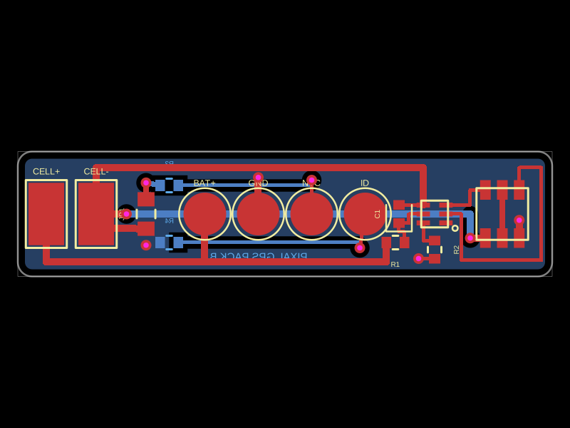 More from this authorpixalynx/pixal-gpsThese designs implement a compact two-layer printed circuit board featuring a battery protection circuitry with cell contact pads and protection ICs, and a wireless charging dock with inductive coil, resonance capacitors, and interface connectors.
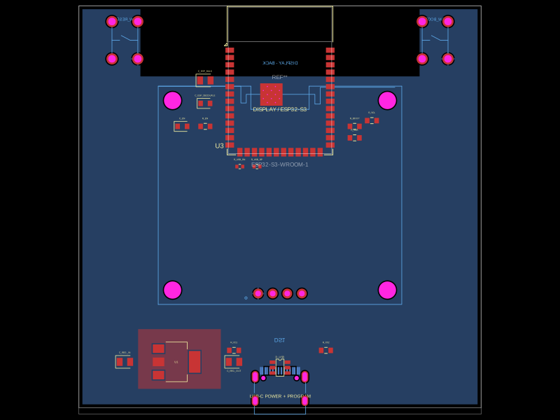 Similar packagegokul/board-v2This design integrates an ESP32-S3 Wi-Fi and Bluetooth module, a USB-C port with power and data circuitry, a USB ESD protection chip, a 3.3V voltage regulator, and an OLED display module on a PCB with associated routing and thermal copper pour layers.
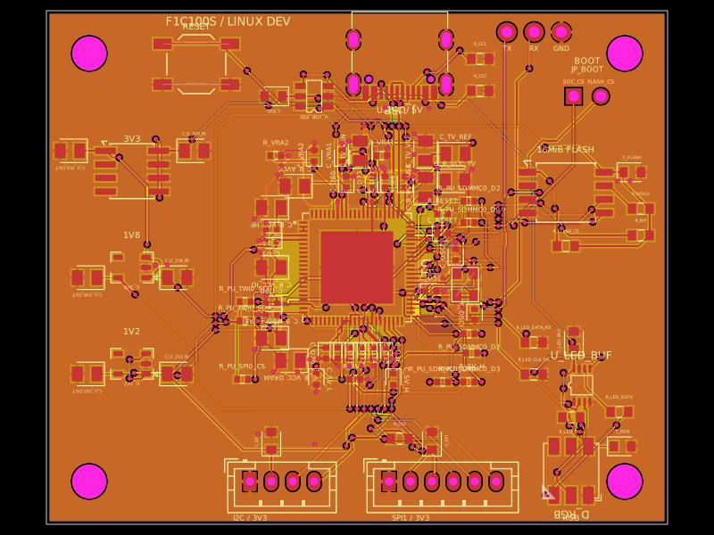 Discover something newseveibar/f1c1990s-dev-boardThis code manages the entire PCB assembly process for a computer hardware module, including component placement, schematic integration, automated routing, copper pouring, and design rule checks, focused on a four-layer carrier board with integrated support components and connectors.