imrishabh18/pcbgolf
These code snippets define detailed PCB footprints for various SMD components, through-hole connectors, and chips, specifying pad locations, shapes, silkscreen outlines, and mechanical outlines for physical placement on a circuit board.
- Version
- 1.4.3
- License
- unset
- Stars
- 0
validation/sd-access-audit.json
{
  "passes": true,
  "revision": "1.4.0",
  "reference": "J2",
  "boardSha256": "1d5a67259402ca55437ba7fea97618a3031cb3573f07de303cb0f32f1cae0d3f",
  "circuitSha256": "ea161c65cae61be08b5769eba53b8ed622e482b009781fc770157f20dac8cd75",
  "pcbRotationDegrees": 270,
  "cadRotationDegrees": 270,
  "cadBodyCenterMm": {
    "x": -29.699999999999996,
    "y": -10.000000000000002,
    "z": 0.8
  },
  "cardAccessDirectionXY": [
    -1,
    0
  ],
  "modelMinXmm": -36.95,
  "boardLeftEdgeXmm": -37.4,
  "housingSetbackMm": 0.45,
  "note": "Outward orientation retained from 1.3.1; socket moved 13.5 mm up and 0.4 mm left. Static CAD/footprint access check; original hinged socket needs lid clearance above the board."
}
Related Packages
 More from this authorimrishabh18/C12084Generated from JLCPCB part number C12084
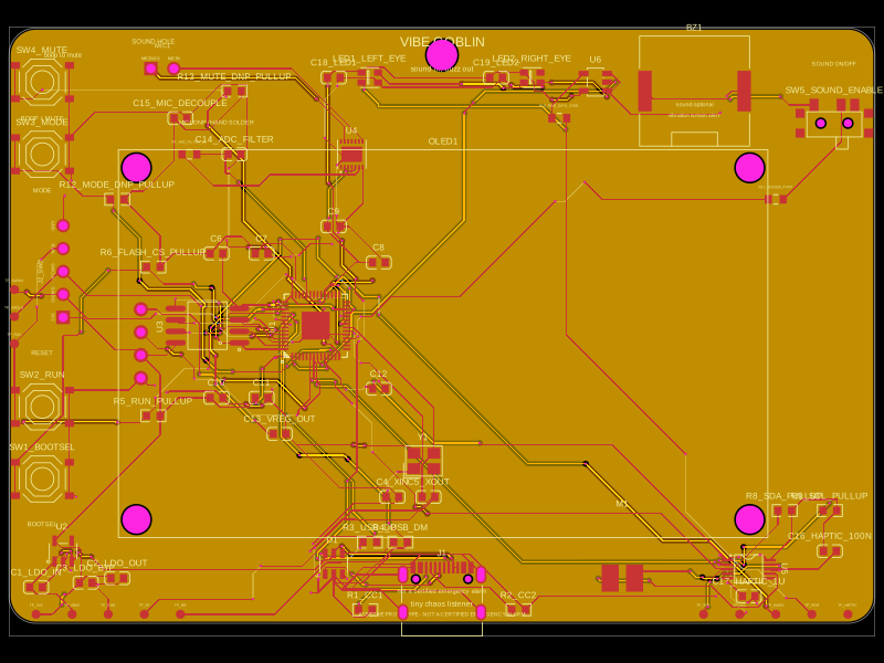 Similar packageAnasSarkiz/vibe_GoblinThese code snippets define various physical electronic components such as ICs, connectors, sensors, LEDs, and chips, specifying their pin layouts, footprint pads, silkscreen markings, courtyard outlines, and 3D CAD models for placement on PCB boards.
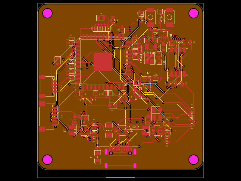 Discover something newtechmannih/trellis-coreThis code defines a detailed electronic hardware schematic and PCB layout for a Linux System-on-Module, incorporating components such as oscillators, power regulators, USB-C connectors, connectors, LEDs, resistors, capacitors, inductors, and integrated circuits, with precise physical footprint and 3D models.