README.md
# PCBGolf in tscircuit

Revision **1.4.1** removes 26 redundant copper segments and trims 52 dangling tails, eliminating **113.31 mm** of unnecessary copper. Pad and via connectivity, USB geometry, power reservations, 4 layers and 990 vias are preserved. All 25 release gates pass; DRC and unconnected-item counts remain zero. See `validation/stub-cleanup-revision.json`. Registry package: [imrishabh18/pcbgolf](https://tscircuit.com/imrishabh18/pcbgolf).

Revision **1.4.0** places **44 populated parts on the underside**, leaving 211 on top, and retains **four copper layers**. The PCB shrinks from **75.7 × 67.5 mm to 75.7 × 56.5 mm**, a **16.03% reduction in actual outline area**. Its complete CAD-estimated score improves from **135,359.09 to 132,298.39** (**2.26% lower**), including the underside parts and **990 vias**. J1 and J2 retain their outward-facing orientation, J3 moves to the new lower edge, and all four mounting holes remain removed. See `validation/two-sided-revision.json`, `validation/release-score-improvement.json`, and `validation/sd-access-audit.json`. Published as [imrishabh18/pcbgolf@1.4.0](https://tscircuit.com/imrishabh18/pcbgolf).

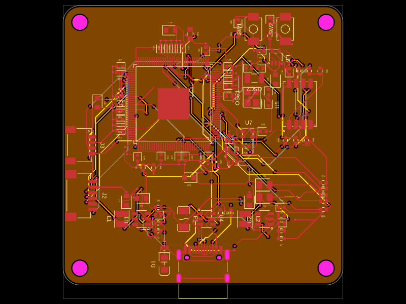
A 75.7 × 56.5 mm, four-layer TypeScript/JSX implementation of [comma.ai's PCBGolf challenge](https://github.com/commaai/PCBGolf). It preserves the 12 V input, 5 V/3.3 V supplies, four switched OBD-C ports, current monitoring, four CAN transceivers, ignition simulation, USB hub/host, STM32H725, microSD, button, and indicators.


| Final release result | Value |
| --- | --- |
| Native remaining connections / airwires / physical DRC errors | **0 / 0 / 0** |
| Copper layers / through vias | **4 / 990** |
| Worst USB physical-contact path skew | **0.999999 mm** (limit 1.25 mm) |
| Populated CAD assembly bounding box | **77.10 × 57.29 × 14.22 mm** |
| Populated CAD assembly volume / contest score | **62,798.39 mm³ / 132,298.39** |
| tscircuit routing / placement DRC errors | **0 / 0** |

The score uses the complete populated assembly: volume in mm³ + 50 × vias + 5,000 × copper layers. The verified layer/via contribution is **69,500**, before assembly volume. Dimensions and score are CAD estimates; the source netlist, native copper and assembly models are checked separately.

Open `kicad/pcbgolf.kicad_pro` in **KiCad 10**. Use `bun run dev` for tscircuit’s PCB and 3D views. `kicad/pcbgolf-assembly.step` contains the assembly. `fabrication/` contains Gerbers, separate plated/nonplated drills, BOM, and positions. The native project includes its footprints and models.

For the tscircuit project, install **Bun** and run from this directory:

```sh
bun install --frozen-lockfile
bun run typecheck
bun run build:placement
bun run build:routed
bun run test:drc
bun run check:drc
bun run render:routed
bun run dev
```

The project pins tscircuit 0.0.2506. The 1.0.0 baseline was checked with a fresh frozen-lockfile installation; that historical receipt is in validation/history/1.0.0/. The two-sided, four-layer 1.4.0 revision passes TypeScript, all eight DRC regression tests and all 25 release gates, including a mandatory score improvement over 1.3.1. Edit `index.circuit.tsx`, `placement.json`, `board-outline.json`, `interface-labels.json`, and `footprints/`. The placement build includes the schematic; the routed build restores checked copper through `saved-autorouter.ts`. Rendered views are `dist/board.png` and `dist/board.svg`. The saved route cache is part of the design and must remain with the source.

**tscircuit 3D models.** `jlcpcb-parts.tsx` imports CAD definitions from the actual `tsci import --jlcpcb` component TSX files in `imports/`. All 255 populated parts now have explicit CAD model URLs; none use bounding-box placeholders. `cad-model-assignments.json` records each model source and its alignment to the retained routed footprint. There are 239 component instances using JLCPCB models (including explicitly identified package-only visual equivalents) and 16 using the original source CAD because exact JLCPCB/EasyEDA model data was unavailable. Visual equivalents do not change the authored MPN, component value, pin mapping, footprint, or routing. The original CAD is retained for J5–J8, L1–L2, D2, LED1, and LED10–LED17. The native assembly envelope/score above still uses the reviewed original assembly models.

Generate tscircuit's own populated 3D snapshot with:

```sh
tsci snapshot dist/route.circuit.json --3d --pcb-only --camera-preset top-left-corner --update
```

The model links are also used by tscircuit's regular 3D view (`bun run dev`). Open `snapshots/tscircuit-3d.png` for the rendered image.

**Source and population.** `upstream/` and `source-data.original.json` preserve [commit 7210bdb](https://github.com/commaai/PCBGolf/tree/7210bdb5049c5b7fdf4900a34928e2736767292a). The reviewed design has **258 components, 191 connected nets, 1,053 logical pins, and 1,068 physical pad/hole records**. Its **255 populated components** have assembly models. The four mechanical mounting holes are removed in `source-removals.json`; all electrical parts remain. C6, C10 and J4 retain the original DNP flags; `source-population.json` records their BOM/position exclusions. The optional J4 model does not enter the populated assembly score.

Declared corrections preserve used functions and mating interfaces:

- U9–U12 use the specified NCS20071SN2T1G five-pin package with function-correct pin numbering.
- U1 uses AP62300TWU-7 for the existing 3.3 V divider; U2 retains AP62300WU-7 for 5 V.
- J3 uses GCT USB4105-GF-A, preserving reversible USB2 Type-C, CC, power, and shield functions. Unused SuperSpeed contacts/redundant aliases are removed. Two ground lands have a 0.015 mm end trim; mechanical holes remain nominal.
- C54–C70 add sixteen 100 nF bypass capacitors and one 10 µF analog-supply capacitor using MPNs and footprints already in the source.

Datasheets, exact pin mappings, and source differences are in `source-corrections.json` , `source-additions.json`, and `source-removals.json`.

**Fabrication and access.** The selected stack is **JLC041611-7628, nominal 1.6 mm (listed finished thickness 1.57 mm), ENIG, green mask**, with 1 oz outer and inner copper. In1 and In2 carry signals and GND fills; every filled ground region belongs to one checked physical ground network. Controlled USB trunks retain continuous adjacent ground coverage. The manufacturer’s 90 Ω calculator target is **9.46 mil width / 6 mil gap**. The retained USB geometry is **9.74 mil / 6 mil** (0.247396 / 0.1524 mm), so its nominal impedance is slightly below that target; the calculator tolerance is not a fabricated-impedance guarantee. Short local neckdowns and fanout transitions are documented in the USB audit. `validation/stackup-impedance.json` records the selected stack and calculation. Ordinary low-current escapes use traces down to **4 mil (0.1016 mm)**; reviewed power paths retain their required copper cross-sections.

Dense signal escapes use **0.40 mm pads / 0.20 mm drills** where needed. Select JLC's **extra-cost option for via diameters below 0.45 mm**. Standard/power-bank vias use 0.45/0.20 mm. See `validation/signal-via-manufacturing.json` and the native manufacturing rules.

J1 faces right, with its mating housing extending 1.4 mm beyond the right edge. Host USB J3 faces the lower edge, with 0.795 mm housing overhang. Both overhangs are included in the assembly score. J5–J8 mate vertically. The microSD socket J2 faces left and sits 0.45 mm inside that edge; its hinged lid requires access from above. Both regulators, their associated power parts and selected small signal components occupy the underside. C6 and C10 retain their DNP status on the bottom, giving 46 bottom footprints and 44 populated bottom parts. J4 remains DNP on top. All four mounting holes are removed, and the vacant upper corners remain chamfered. Silkscreen identifies OBD-C 1–4, host USB, and 12 V input. The bottom components add 1.585 mm to assembly height, and the 13 extra vias cost 650 points; these effects reduce the score benefit relative to the area saving.

**Changing placement requires new routing.** The saved-route adapter rejects mismatched pins/positions. Rebuild placement, reroute, and recheck USB and power/ground reservations. After checking the revised native board, refresh its cache with KiCad's Python:

```sh
"$KICAD_PYTHON" scripts/import-routes.py \
  --board revised.kicad_pcb --circuit-json dist/placement.circuit.json \
  --output-board rebuilt/verified.kicad_pcb --output-cache rebuilt/raw-cache.json
python3 scripts/coalesce-route-cache.py rebuilt/raw-cache.json routed-cache.json
bun run build:routed
```

Set `KICAD_PYTHON` to Python with `pcbnew`. General routing helpers also require local Freerouting and Java 21. Routing phases restore the accepted four-layer copper; bounded routing helpers limit added vias per connection. Six-layer reservation files are retained for the layer-specific legacy validators; `layer-stack.json` and the physical four-layer ground audit select the current rules. USB and power paths retain explicit reservations. Adopt the checked native board and refreshed cache together.

**Release validation.** With the final native board and route cache in their canonical paths:

```sh
bun run export:release
bun run package:release
```

The exporter locates KiCad on macOS; elsewhere, pass `--kicad-python` and `--kicad-cli` to `scripts/export-release.py`.

Export gates check source/schematic nets, exact pad/copper parity, native DRC/connectivity, USB/reference planes, reviewed In1 crossings, power/ground paths, manufacturing, and assembly models. The checked-in Bun patch for `@tscircuit/checks@0.0.189` corrects rounded-pad distances, distinguishes via-to-pad copper spacing from SMT pad spacing, and follows physical contacts through branches, barrels, and filled copper regions. The live tscircuit build now emits zero DRC errors. No errors are filtered or suppressed, and all design clearances are retained. Revision 1.4.0 reroutes the relocated parts, shortens and tunes the host USB pair while retaining its six vias, and preserves the exact copper of the other ten USB nets. `validation/usb-pairs/v5/` contains the accepted current USB evidence. Final audits verify each contact path and continuous ground coverage beneath the controlled bottom-layer trunks. Historical revision receipts remain under `validation/history/` or identify their original board hashes. `bun run test:drc` checks valid geometry and deliberate faults, and `bun run check:drc` reruns the routing/placement checks against the built Circuit JSON. The original 734 reports are retained as historical evidence in `validation/drc-fix/before.runtime-findings.json`. Native library-identity and protected-tail warnings remain recorded separately. `validation/release-manifest.json` binds files by SHA256. Verified packaging produces `../pcbgolf-tscircuit.zip` and `validation/package-manifest.json`.

The input limit is **5 A aggregate**; each channel's nominal protection threshold is approximately 3.18 A. Four simultaneous full-threshold loads exceed the input rating. The board **has not been fabricated or bench-tested**: power, thermal/transient behavior, USB, CAN, and microSD require hardware validation. No fabrication order or contest submission has been made.