0hmX/simplified-am62l-computer
This code defines components and scripts for physically representing and routing high-speed DDR memory signals, power lines, and ground planes on an 8-layer PCB with detailed pin assignments, copper pours, and precise via and trace layouts based on TI EVM reference data.
- Version
- 1.0.16
- License
- unset
- Stars
- 0
imports/USB4125_GF_A_0190/USB4125_GF_A_0190.tsx
import objPath from "./USB4125_GF_A_0190.obj"
import type { ChipProps } from "@tscircuit/props"

const pinLabels = {
  pin7: ["pin7"],
  pin8: ["pin7_alt1"],
  pin9: ["pin7_alt1"],
  pin10: ["pin7_alt1"],
  pin11: ["A12"],
  pin12: ["A9"],
  pin13: ["B5"],
  pin14: ["A5"],
  pin15: ["B9"],
  pin16: ["B12"]
} as const

export const USB4125_GF_A_0190 = (props: ChipProps<typeof pinLabels>) => {
  return (
    <chip
      pinLabels={pinLabels}
      supplierPartNumbers={{
  "jlcpcb": [
    "C5246813"
  ]
}}
      manufacturerPartNumber="USB4125_GF_A_0190"
      footprint={<footprint>
        <platedhole  portHints={["pin7"]} pcbX="-4.319905mm" pcbY="1.5850426mm" holeWidth="0.5999988mm" holeHeight="1.1999976mm" outerWidth="1.0999978mm" outerHeight="1.6999966mm" shape="pill" />
<platedhole  portHints={["pin8"]} pcbX="4.319905mm" pcbY="1.5850426mm" holeWidth="0.5999988mm" holeHeight="1.1999976mm" outerWidth="1.0999978mm" outerHeight="1.6999966mm" shape="pill" />
<platedhole  portHints={["pin9"]} pcbX="-4.319905mm" pcbY="-2.2150514mm" holeWidth="0.5999988mm" holeHeight="1.1999976mm" outerWidth="1.0999978mm" outerHeight="1.6999966mm" shape="pill" />
<platedhole  portHints={["pin10"]} pcbX="4.319905mm" pcbY="-2.2150514mm" holeWidth="0.5999988mm" holeHeight="1.1999976mm" outerWidth="1.0999978mm" outerHeight="1.6999966mm" shape="pill" />
<smtpad portHints={["pin11"]} pcbX="2.750185mm" pcbY="1.6650526mm" width="0.7999984mm" height="1.1999976mm" shape="rect" />
<smtpad portHints={["pin12"]} pcbX="1.520063mm" pcbY="1.6650526mm" width="0.6999986mm" height="1.1999976mm" shape="rect" />
<smtpad portHints={["pin13"]} pcbX="0.499999mm" pcbY="1.6650526mm" width="0.6999986mm" height="1.1999976mm" shape="rect" />
<smtpad portHints={["pin14"]} pcbX="-0.499999mm" pcbY="1.6650526mm" width="0.6999986mm" height="1.1999976mm" shape="rect" />
<smtpad portHints={["pin15"]} pcbX="-1.520063mm" pcbY="1.6650526mm" width="0.6999986mm" height="1.1999976mm" shape="rect" />
<smtpad portHints={["pin16"]} pcbX="-2.750185mm" pcbY="1.6650526mm" width="0.7999984mm" height="1.1999976mm" shape="rect" />
<silkscreenpath route={[{"x":-3.381222600000001,"y":1.9899948000000904},{"x":-3.5458653999997978,"y":1.9899948000000904}]} />
<silkscreenpath route={[{"x":-2.1011387999999442,"y":1.9899948000000904},{"x":-2.1189441999998735,"y":1.9899948000000904}]} />
<silkscreenpath route={[{"x":2.1189696000001277,"y":1.9899948000000904},{"x":2.1011387999999442,"y":1.9899948000000904}]} />
<silkscreenpath route={[{"x":3.545865400000025,"y":1.9899948000000904},{"x":3.381248000000028,"y":1.9899948000000904}]} />
<silkscreenpath route={[{"x":4.4699935999999525,"y":-1.14850540000009},{"x":4.4699935999999525,"y":0.5184965999999349}]} />
<silkscreenpath route={[{"x":-4.4699935999999525,"y":-3.2815974000000097},{"x":-4.4699935999999525,"y":-4.8149954000000434},{"x":4.4699935999999525,"y":-4.8149954000000434},{"x":4.4699935999999525,"y":-3.2815974000000097}]} />
<silkscreenpath route={[{"x":-4.4699935999999525,"y":0.5184965999999349},{"x":-4.4699935999999525,"y":-1.14850540000009}]} />
<silkscreentext text="{NAME}" pcbX="-0.005207mm" pcbY="3.4232426mm" anchorAlignment="center" fontSize="1mm" />
<courtyardoutline outline={[{"x":-5.119306999999935,"y":2.6732425999999805},{"x":5.108892999999966,"y":2.6732425999999805},{"x":5.108892999999966,"y":-5.192757400000005},{"x":-5.119306999999935,"y":-5.192757400000005},{"x":-5.119306999999935,"y":2.6732425999999805}]} />
      </footprint>}
      cadModel={{
        objUrl: objPath,
        pcbRotationOffset: 0,
        modelOriginPosition: { x: 0, y: 1.3629957000000559, z: -0.0000020000000000575113 },
      }}
      {...props}
    />
  )
}
Related Packages
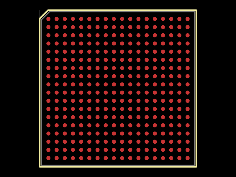 More from this author0hmX/am3352-zcz-footprintThis code defines the physical footprint and pin layout for an 18x18 ball grid array (BGA) package of a Texas Instruments AM3352 microprocessor, including pad positions and outline drawing commands for PCB design.
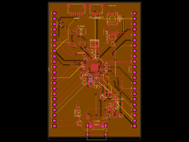 Similar packageabse/rp2350-mcu-boardThis code defines a compact, four-layer PCB hardware layout for the Raspberry Pi RP2350A microcontroller module, including the main IC, power regulation, USB-C connector, STM32-compatible headers, and associated passive components, with detailed component footprints, net connections, and copper pour zones for powering and ground references.
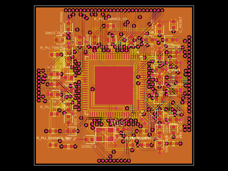 Discover something newastra/f1c100sThe code defines the physical pin layout, labels, and footprint for the F1C100S system-on-chip (SoC) component used in electronic devices.