0hmX/simplified-am62l-computer
This code defines components and scripts for physically representing and routing high-speed DDR memory signals, power lines, and ground planes on an 8-layer PCB with detailed pin assignments, copper pours, and precise via and trace layouts based on TI EVM reference data.
- Version
- 1.0.16
- License
- unset
- Stars
- 0
imports/C1005X5R1A335KTJ00E.tsx
import type { CapacitorProps } from "@tscircuit/props"

const pinLabels = {
  pin1: ["pin1"],
  pin2: ["pin2"]
} as const

export const C1005X5R1A335KTJ00E = (props: Omit<CapacitorProps, "capacitance">) => {
  return (
    <capacitor capacitance="3.3uF"
      symbol={false ? (
        <symbol>
          <schematicpath points={[{"x":-0.508,"y":-2.032},{"x":-0.508,"y":2.032}]} strokeWidth={0.254} strokeColor="#A00000" />
          <port name="pin1" pinNumber={1} aliases={["1"]} direction="left" schX={-5.08} schY={0} schStemLength={2.54} />
          <schematicpath points={[{"x":2.54,"y":0},{"x":0.508,"y":0}]} strokeWidth={0.254} strokeColor="#A00000" />
          <schematicpath points={[{"x":0.508,"y":2.032},{"x":0.508,"y":-2.032}]} strokeWidth={0.254} strokeColor="#A00000" />
          <port name="pin2" pinNumber={2} aliases={["2"]} direction="right" schX={5.08} schY={0} schStemLength={2.54} />
          <schematicpath points={[{"x":-0.508,"y":0},{"x":-2.54,"y":0}]} strokeWidth={0.254} strokeColor="#A00000" />
        </symbol>
      ) : undefined}
      supplierPartNumbers={{
  "jlcpcb": [
    "C695126"
  ]
}}
      manufacturerPartNumber="C1005X5R1A335KTJ00E"
      footprint={<footprint>
        <smtpad portHints={["pin2"]} pcbX="0.420116mm" pcbY="0mm" width="0.499999mm" height="0.540004mm" shape="rect" />
<smtpad portHints={["pin1"]} pcbX="-0.420116mm" pcbY="0mm" width="0.499999mm" height="0.540004mm" shape="rect" />
<silkscreenpath route={[{"x":-0.721385400000031,"y":0.49753519999990203},{"x":-0.22138640000002852,"y":0.49753519999990203}]} />
<silkscreenpath route={[{"x":-0.8738108000000011,"y":-0.34724340000002485},{"x":-0.8738108000000011,"y":0.3451606000000993}]} />
<silkscreenpath route={[{"x":-0.22138640000002852,"y":-0.4996433999999681},{"x":-0.721385400000031,"y":-0.4996433999999681}]} />
<silkscreenpath route={[{"x":0.7213853999999174,"y":-0.4975097999999889},{"x":0.22138639999991483,"y":-0.4975097999999889}]} />
<silkscreenpath route={[{"x":0.22138639999991483,"y":0.49961800000005496},{"x":0.7213853999999174,"y":0.49961800000005496}]} />
<silkscreenpath route={[{"x":0.8738108000000011,"y":0.34726880000005167},{"x":0.8738108000000011,"y":-0.3451606000000993}]} />
<silkscreenpath route={[{"x":0.7213853999999174,"y":0.4996433999998544},{"x":0.829148473452733,"y":0.4550064734527268},{"x":0.8737853999998606,"y":0.34724340000002485}]} />
<silkscreenpath route={[{"x":0.8737853999998606,"y":-0.3451606000000993},{"x":0.829148473452733,"y":-0.4529236734526876},{"x":0.7213853999999174,"y":-0.49756059999992885}]} />
<silkscreenpath route={[{"x":-0.721385400000031,"y":-0.4996433999997407},{"x":-0.829148473452733,"y":-0.45500647345261314},{"x":-0.8737853999999743,"y":-0.34724340000002485}]} />
<silkscreenpath route={[{"x":-0.8737853999999743,"y":0.3451606000000993},{"x":-0.829148473452733,"y":0.45292367345280127},{"x":-0.721385400000031,"y":0.49756060000004254}]} />
<silkscreentext text="{NAME}" pcbX="0.0127mm" pcbY="1.508mm" anchorAlignment="center" fontSize="1mm" />
<courtyardoutline outline={[{"x":-1.1136000000000195,"y":0.7580000000000382},{"x":1.1389999999998963,"y":0.7580000000000382},{"x":1.1389999999998963,"y":-0.7326000000000477},{"x":-1.1136000000000195,"y":-0.7326000000000477},{"x":-1.1136000000000195,"y":0.7580000000000382}]} />
      </footprint>}
      cadModel={{
        objUrl: "https://modelcdn.tscircuit.com/easyeda_models/assets/C695126.obj?uuid=32fe2cf9314f444ca2785a33c2db7189",
        stepUrl: "https://modelcdn.tscircuit.com/easyeda_models/assets/C695126.step?uuid=32fe2cf9314f444ca2785a33c2db7189",
        pcbRotationOffset: 0,
        modelOriginPosition: { x: 0, y: -0.000012700000070253736, z: -0.25 },
      }}
      {...props}
    />
  )
}
Related Packages
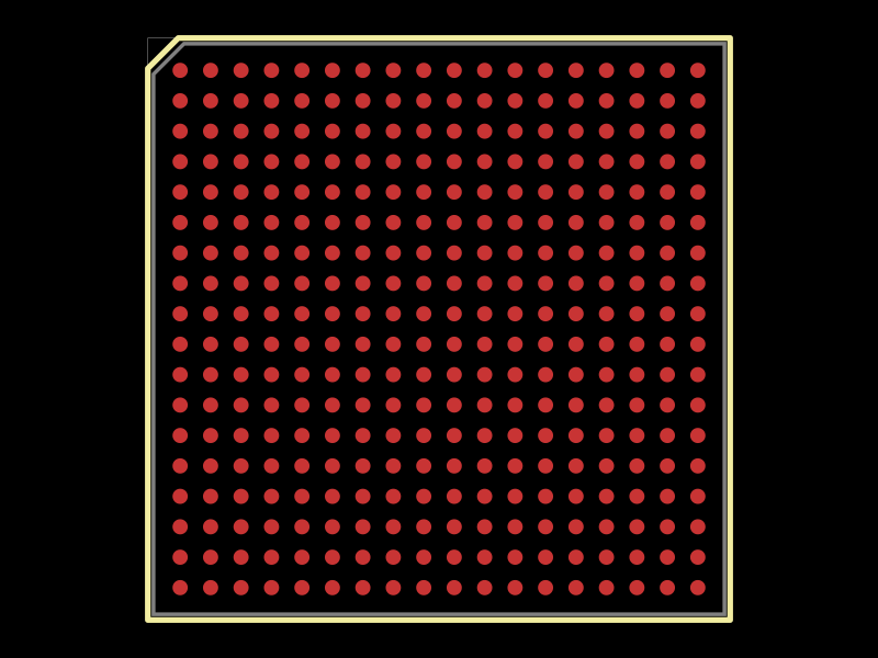 More from this author0hmX/am3352-zcz-footprintThis code defines the physical footprint and pin layout for an 18x18 ball grid array (BGA) package of a Texas Instruments AM3352 microprocessor, including pad positions and outline drawing commands for PCB design.
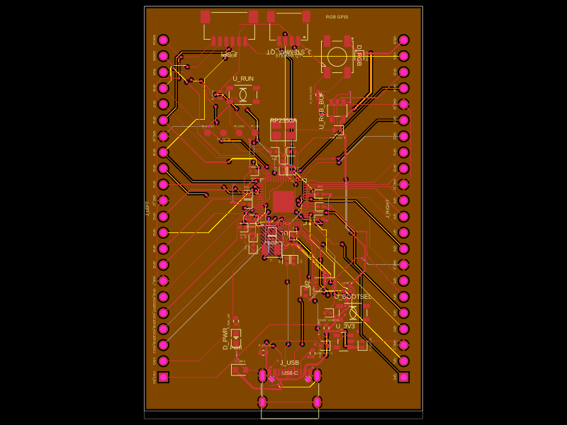 Similar packageabse/rp2350-mcu-boardThis code defines a compact, four-layer PCB hardware layout for the Raspberry Pi RP2350A microcontroller module, including the main IC, power regulation, USB-C connector, STM32-compatible headers, and associated passive components, with detailed component footprints, net connections, and copper pour zones for powering and ground references.
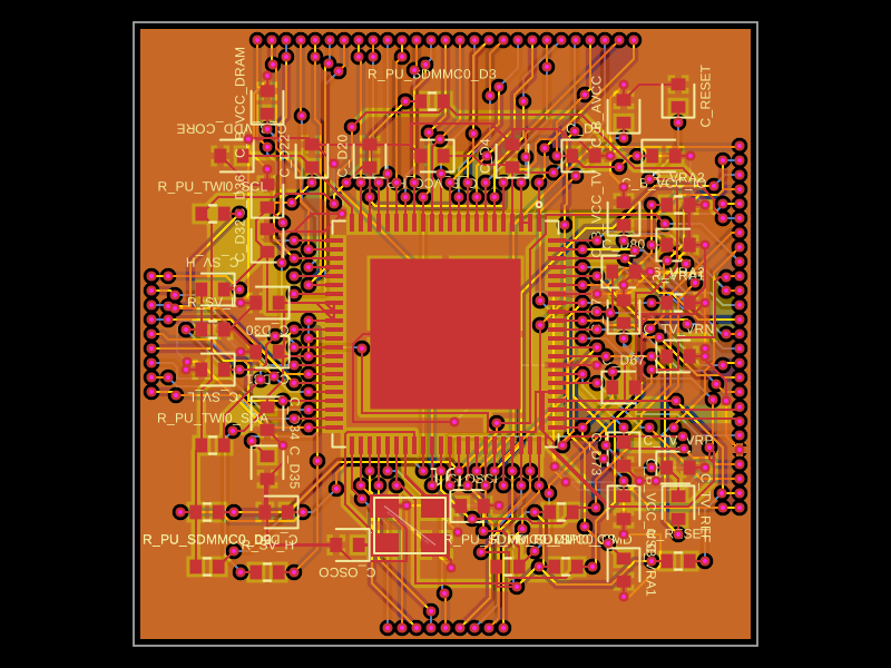 Discover something newastra/f1c100sThe code defines the physical pin layout, labels, and footprint for the F1C100S system-on-chip (SoC) component used in electronic devices.