tscircuit/boosters
This code defines PCB schematics, footprints, and 3D CAD models for various integrated circuits, connectors, sensors, and electronic components used in TI booster packs and modules.
- Version
- 0.1.19
- License
- unset
- Stars
- 0
boostxl-tlv8544pir/index.circuit.tsx
PCB

Schematic

import { A_1N4148X_TP } from "./imports/A_1N4148X_TP";
import { A_19_213_Y2C_CQ2R2L_3T_CY_ } from "./imports/A_19_213_Y2C_CQ2R2L_3T_CY_";
import { A_19_217_G7C_AN1P2_6T } from "./imports/A_19_217_G7C_AN1P2_6T";
import { A_19_217_R6C_AL1M2VY_3T } from "./imports/A_19_217_R6C_AL1M2VY_3T";
import { A_5001 } from "./imports/A_5001";
import { BLM18HE152SN1D } from "./imports/BLM18HE152SN1D";
import { DZ254S_11_02_48 } from "./imports/DZ254S_11_02_48";
import { INA226AIDGSR } from "./imports/INA226AIDGSR";
import { IRA_S210ST01 } from "./imports/IRA_S210ST01";
import { SSQ_110_03_G_D } from "./imports/SSQ_110_03_G_D";
import { TLV333IDBVR } from "./imports/TLV333IDBVR";
import { TLV8544PWR } from "./imports/TLV8544PWR";
/**
* Keys preserve TI's SNOU148A terminology. Compact net/trace names keep the
* rendered labels inside their schematic sections without changing connectivity.
*/
const N = {
GND: "net.GND",
V5_LPD: "net.V5_LPD",
V3P3_LPD: "net.V33_LPD",
V5: "net.V5_FILT",
V3P3: "net.V33_FILT",
V3P3_TLV: "net.V33_TLV",
V3P3_REF: "net.V33_REF",
V3P3_INA: "net.V33_INA",
V_TLV: "net.V_TLV",
V_PIR: "net.V_PIR",
PIR_VIN1: "net.PIRIN",
PIR_VOUT_RAW: "net.RAW",
PIR_VO: "net.PIRVO",
U1A_INV: "net.AINV",
U1A_AC_RETURN: "net.AC",
U1A_OUT: "net.AOUT",
INTERSTAGE: "net.INTER",
U1B_INV: "net.BINV",
U1B_REF: "net.BREF",
U1B_OUT: "net.BOUT",
PIR_SIGNAL_BUS: "net.BUS",
REF_HIGH: "net.HI",
REF_MID: "net.MID",
REF_LOW: "net.LO",
U1C_OUT: "net.COUT",
U1D_OUT: "net.DOUT",
BUFFER_OUT: "net.BUF",
// tscircuit net identifiers cannot begin with a digit; this is TI's 1STAG_AOUT.
FIRST_STAGE_AOUT: "net.STG1_OUT",
PIR_SGL_AOUT: "net.PIR_SGL",
PIR_OUT_HI: "net.PIR_HI",
PIR_OUT_LO: "net.PIR_LO",
I2C_CS: "net.I2C_CS",
I2C_SCL: "net.I2C_SCL",
I2C_SDA: "net.I2C_SDA",
OLED: "net.OLED",
RLED: "net.RLED",
YLED: "net.YLED",
} as const;
export default function Circuit() {
return (
<board
name="BOOSTXL_TLV8544PIR"
width="60.96mm"
height="50.8mm"
outline={[
{ x: -30.48, y: -22.86 },
{ x: -27.94, y: -25.4 },
{ x: 27.94, y: -25.4 },
{ x: 30.48, y: -22.86 },
{ x: 30.48, y: 22.86 },
{ x: 27.94, y: 25.4 },
{ x: -27.94, y: 25.4 },
{ x: -30.48, y: 22.86 },
]}
solderMaskColor="red"
silkscreenColor="white"
defaultTraceWidth="0.2mm"
minViaHoleDiameter="0.3mm"
minViaPadDiameter="0.45mm"
autorouter={{
preset: "auto_local",
local: true,
traceClearance: "0.15mm",
}}
autorouterEffortLevel="2x"
autorouterVersion="v6"
>
<schematicsheet
name="PIR Signal Conditioning"
displayName="PIR Sensor Signal Conditioning"
sheetIndex={1}
/>
<schematicsheet
name="LaunchPad Interface"
displayName="LaunchPad Interface and Headers"
sheetIndex={2}
/>
<schematicsheet
name="User Status LEDs"
displayName="User Status LEDs"
sheetIndex={3}
/>
<schematicsheet
name="Power Rail Distribution"
displayName="Power Filtering and Rail Distribution"
sheetIndex={4}
/>
<schematicsheet
name="INA226 Current Monitor"
displayName="INA226 Current Monitor and Buffer"
sheetIndex={5}
/>
<group
name="LAUNCHPAD_INTERFACE"
schSheetName="LaunchPad Interface"
schX={7}
schY={2}
pcbX={0}
pcbY={0}
>
<schematicsection
name="LAUNCHPAD_CONNECTORS"
displayName=""
sectionTitleFontSize="0.24mm"
/>
<schematictext
text="LaunchPad Headers"
schX={-13.6}
schY={0.9}
fontSize={0.22}
anchor="center_left"
/>
{/* LaunchPad BoosterPack headers. Exact Samtec female sockets imported from
JLCPCB and mounted on the bottom so the BoosterPack mates downward. */}
<SSQ_110_03_G_D
name="J1"
layer="bottom"
schSectionName="LAUNCHPAD_CONNECTORS"
schX={-9}
schY={-2}
schWidth="3.2mm"
pcbX={-17.78}
pcbY={5.08}
pcbRotation={90}
connections={{
pin1: N.V3P3_LPD,
pin2: N.V5_LPD,
pin3: N.FIRST_STAGE_AOUT,
pin4: N.GND,
pin10: N.PIR_OUT_HI,
pin11: N.PIR_SGL_AOUT,
pin12: N.PIR_OUT_LO,
pin14: N.I2C_CS,
pin16: N.OLED,
pin17: N.I2C_SCL,
pin18: N.RLED,
pin19: N.I2C_SDA,
pin20: N.YLED,
}}
/>
<SSQ_110_03_G_D
name="J2"
layer="bottom"
schSectionName="LAUNCHPAD_CONNECTORS"
schX={-1.8}
schY={-2}
schWidth="3.2mm"
pcbX={25.4}
pcbY={5.08}
pcbRotation={90}
connections={{ pin20: N.GND }}
/>
{/* LaunchPad signal filtering. */}
<capacitor
name="C1"
schSectionName="LAUNCHPAD_CONNECTORS"
schX={-13.3}
schY={-0.7}
schRotation="270deg"
manufacturerPartNumber="GRM188R71H103KA01D"
supplierPartNumbers={{ jlcpcb: ["C77053"] }}
capacitance="0.01uF"
footprint="0603"
pcbX={-12.5}
pcbY={8}
pcbRotation={0}
connections={{ pin1: N.PIR_OUT_HI, pin2: N.GND }}
/>
<capacitor
name="C2"
schSectionName="LAUNCHPAD_CONNECTORS"
schX={-5.2}
schY={-0.7}
schRotation="270deg"
manufacturerPartNumber="GRM188R71H103KA01D"
supplierPartNumbers={{ jlcpcb: ["C77053"] }}
capacitance="0.01uF"
footprint="0603"
pcbX={-25.8}
pcbY={14.5}
pcbRotation={90}
connections={{ pin1: N.FIRST_STAGE_AOUT, pin2: N.GND }}
/>
<capacitor
name="C3"
schSectionName="LAUNCHPAD_CONNECTORS"
schX={-13.3}
schY={-3}
schRotation="270deg"
manufacturerPartNumber="GRM188R71H103KA01D"
supplierPartNumbers={{ jlcpcb: ["C77053"] }}
capacitance="0.01uF"
footprint="0603"
pcbX={-12.8}
pcbY={4.2}
pcbRotation={90}
connections={{ pin1: N.PIR_OUT_LO, pin2: N.GND }}
/>
<capacitor
name="C4"
schSectionName="LAUNCHPAD_CONNECTORS"
schX={-5.2}
schY={-3}
schRotation="270deg"
manufacturerPartNumber="GRM188R71H103KA01D"
supplierPartNumbers={{ jlcpcb: ["C77053"] }}
capacitance="0.01uF"
footprint="0603"
pcbX={-25.8}
pcbY={5}
pcbRotation={90}
connections={{ pin1: N.PIR_SGL_AOUT, pin2: N.GND }}
/>
</group>
<group
name="PIR_SIGNAL_CHAIN"
schSheetName="PIR Signal Conditioning"
schY={-5.5}
pcbX={0}
pcbY={0}
>
<schematicsection
name="PIR_SIGNAL_CONDITIONING"
displayName=""
sectionTitleFontSize="0.24mm"
/>
<schematictext
text="PIR Sensor Signal Conditioning"
schX={-13.6}
schY={10.2}
fontSize={0.24}
anchor="center_left"
/>
{/* Murata's supported analog PIR sensor. Its exact JLCPCB footprint is
retained because the best footprinter match was only 13.87%. */}
<IRA_S210ST01
name="A1"
schSectionName="PIR_SIGNAL_CONDITIONING"
schX={-6.2}
schY={6.2}
schWidth="2.2mm"
schHeight="1.6mm"
schPinArrangement={{
leftSide: ["d"],
rightSide: ["s"],
bottomSide: ["g"],
}}
pcbX={20.5}
pcbY={-17}
connections={{
d: N.PIR_VIN1,
s: N.PIR_VOUT_RAW,
g: N.GND,
}}
/>
<resistor
name="R12"
schSectionName="PIR_SIGNAL_CONDITIONING"
schX={-13.2}
schY={7.8}
schRotation="270deg"
manufacturerPartNumber="RC0603FR-07619KL"
supplierPartNumbers={{ jlcpcb: ["C245988"] }}
resistance="619kohm"
footprint="0603"
pcbX={-2.5}
pcbY={-17.5}
pcbRotation={0}
connections={{ pin1: N.V_PIR, pin2: N.PIR_VIN1 }}
/>
<capacitor
name="C10"
schSectionName="PIR_SIGNAL_CONDITIONING"
schX={-13}
schY={4}
schRotation="270deg"
manufacturerPartNumber="CGA1206X5R107M100NT"
supplierPartNumbers={{ jlcpcb: ["C6119961"] }}
capacitance="100uF"
footprint="1206"
pcbX={-10}
pcbY={-20.5}
pcbRotation={90}
connections={{ pin1: N.PIR_VIN1, pin2: N.GND }}
/>
<capacitor
name="C11"
schSectionName="PIR_SIGNAL_CONDITIONING"
schX={-11.7}
schY={4}
schRotation="270deg"
manufacturerPartNumber="GRM188R60J106ME47D"
supplierPartNumbers={{ jlcpcb: ["C77041"] }}
capacitance="10uF"
footprint="0603"
pcbX={-6.5}
pcbY={-20.5}
pcbRotation={90}
connections={{ pin1: N.PIR_VIN1, pin2: N.GND }}
/>
<capacitor
name="C12"
schSectionName="PIR_SIGNAL_CONDITIONING"
schX={-10.4}
schY={4}
schRotation="270deg"
manufacturerPartNumber="C1608X7R1C105KT000N"
supplierPartNumbers={{ jlcpcb: ["C76617"] }}
capacitance="1uF"
footprint="0603"
pcbX={-4}
pcbY={-20.5}
pcbRotation={90}
connections={{ pin1: N.PIR_VIN1, pin2: N.GND }}
/>
<capacitor
name="C13"
schSectionName="PIR_SIGNAL_CONDITIONING"
schX={-9.1}
schY={4}
schRotation="270deg"
manufacturerPartNumber="GRM188R71E104KA01D"
supplierPartNumbers={{ jlcpcb: ["C77050"] }}
capacitance="0.1uF"
footprint="0603"
pcbX={-1.5}
pcbY={-20.5}
pcbRotation={90}
connections={{ pin1: N.PIR_VIN1, pin2: N.GND }}
/>
<capacitor
name="C14"
schSectionName="PIR_SIGNAL_CONDITIONING"
schX={-7.8}
schY={4}
schRotation="270deg"
manufacturerPartNumber="GRM188R71H103KA01D"
supplierPartNumbers={{ jlcpcb: ["C77053"] }}
capacitance="0.01uF"
footprint="0603"
pcbX={1}
pcbY={-20.5}
pcbRotation={90}
connections={{ pin1: N.PIR_VIN1, pin2: N.GND }}
/>
<capacitor
name="C15"
schSectionName="PIR_SIGNAL_CONDITIONING"
schX={-6.5}
schY={4}
schRotation="270deg"
manufacturerPartNumber="GRM1885C1H102JA01D"
supplierPartNumbers={{ jlcpcb: ["C77026"] }}
capacitance="1000pF"
footprint="0603"
pcbX={3.5}
pcbY={-20.5}
pcbRotation={90}
connections={{ pin1: N.PIR_VIN1, pin2: N.GND }}
/>
<capacitor
name="C16"
schSectionName="PIR_SIGNAL_CONDITIONING"
schX={-5.2}
schY={4}
schRotation="270deg"
manufacturerPartNumber="GRM1885C1H101JA01D"
supplierPartNumbers={{ jlcpcb: ["C71664"] }}
capacitance="100pF"
footprint="0603"
pcbX={6}
pcbY={-20.5}
pcbRotation={90}
connections={{ pin1: N.PIR_VIN1, pin2: N.GND }}
/>
{/* Quad nanopower op-amp: two gain/filter stages plus window comparators. */}
<TLV8544PWR
name="U1"
schSectionName="PIR_SIGNAL_CONDITIONING"
noSchematicRepresentation
pcbX={14.5}
pcbY={-0.5}
pcbRotation={90}
connections={{
OUT_A: N.U1A_OUT,
IN_A_NEG: N.U1A_INV,
IN_A_POS: N.PIR_VO,
V_POS: N.V_TLV,
IN_B_POS: N.U1B_REF,
IN_B_NEG: N.U1B_INV,
OUT_B: N.U1B_OUT,
OUT_C: N.U1C_OUT,
IN_C_NEG: N.REF_HIGH,
IN_C_POS: N.PIR_SIGNAL_BUS,
V_NEG: N.GND,
IN_D_POS: N.REF_LOW,
IN_D_NEG: N.PIR_SIGNAL_BUS,
OUT_D: N.U1D_OUT,
}}
/>
{/* Native multi-unit schematic projections keep the exact imported U1
package on the PCB while drawing the four op-amps like TI does. */}
<schematicsymbol
name="U1A"
schSectionName="PIR_SIGNAL_CONDITIONING"
displayName="U1A"
chipRef=".U1"
symbolName="opamp_with_power"
schX={-2.2}
schY={6.2}
connections={{
inp1: ".U1 > .IN_A_POS",
inp2: ".U1 > .IN_A_NEG",
out: ".U1 > .OUT_A",
"V+": ".U1 > .V_POS",
"V-": ".U1 > .V_NEG",
}}
/>
<schematicsymbol
name="U1B"
schSectionName="PIR_SIGNAL_CONDITIONING"
displayName="U1B"
chipRef=".U1"
symbolName="opamp_with_power"
schX={4.2}
schY={6.2}
connections={{
inp1: ".U1 > .IN_B_POS",
inp2: ".U1 > .IN_B_NEG",
out: ".U1 > .OUT_B",
"V+": ".U1 > .V_POS",
"V-": ".U1 > .V_NEG",
}}
/>
<schematicsymbol
name="U1C"
schSectionName="PIR_SIGNAL_CONDITIONING"
displayName="U1C"
chipRef=".U1"
symbolName="opamp_with_power"
schX={11.6}
schY={9}
connections={{
inp1: ".U1 > .IN_C_POS",
inp2: ".U1 > .IN_C_NEG",
out: ".U1 > .OUT_C",
"V+": ".U1 > .V_POS",
"V-": ".U1 > .V_NEG",
}}
/>
<schematicsymbol
name="U1D"
schSectionName="PIR_SIGNAL_CONDITIONING"
displayName="U1D"
chipRef=".U1"
symbolName="opamp_with_power"
schX={11.6}
schY={5.2}
connections={{
inp1: ".U1 > .IN_D_POS",
inp2: ".U1 > .IN_D_NEG",
out: ".U1 > .OUT_D",
"V+": ".U1 > .V_POS",
"V-": ".U1 > .V_NEG",
}}
/>
<resistor
name="R14"
schSectionName="PIR_SIGNAL_CONDITIONING"
schX={-4.3}
schY={6.2}
manufacturerPartNumber="0603WAF0000T5E"
supplierPartNumbers={{ jlcpcb: ["C21189"] }}
resistance="0ohm"
footprint="0603"
pcbX={25}
pcbY={-10}
pcbRotation={0}
connections={{ pin1: N.PIR_VOUT_RAW, pin2: N.PIR_VO }}
/>
<resistor
name="R16"
schSectionName="PIR_SIGNAL_CONDITIONING"
schX={-3.7}
schY={3.7}
schRotation="270deg"
manufacturerPartNumber="1RC0603F1304"
supplierPartNumbers={{ jlcpcb: ["C54531191"] }}
resistance="1.30Mohm"
footprint="0603"
pcbX={11}
pcbY={-16}
pcbRotation={90}
connections={{ pin1: N.PIR_VO, pin2: N.GND }}
/>
<resistor
name="R6"
schSectionName="PIR_SIGNAL_CONDITIONING"
schX={-4.5}
schY={8.3}
schRotation="270deg"
manufacturerPartNumber="1RC0603F6811"
supplierPartNumbers={{ jlcpcb: ["C54531559"] }}
resistance="6.81kohm"
footprint="0603"
pcbX={15}
pcbY={-9.5}
pcbRotation={0}
connections={{ pin1: N.U1A_INV, pin2: N.U1A_AC_RETURN }}
/>
<capacitor
name="C5"
schSectionName="PIR_SIGNAL_CONDITIONING"
schX={-4.5}
schY={9.6}
schRotation="270deg"
manufacturerPartNumber="C2012X5R1A336MTJ00E"
supplierPartNumbers={{ jlcpcb: ["C342635"] }}
capacitance="33uF"
footprint="0805"
pcbX={18}
pcbY={-9.5}
pcbRotation={90}
connections={{ pin1: N.U1A_AC_RETURN, pin2: N.GND }}
/>
<resistor
name="R9"
schSectionName="PIR_SIGNAL_CONDITIONING"
schX={-2.2}
schY={8.4}
manufacturerPartNumber="1RC0603F1504"
supplierPartNumbers={{ jlcpcb: ["C54531218"] }}
resistance="1.50Mohm"
footprint="0603"
pcbX={10}
pcbY={-9}
pcbRotation={0}
connections={{ pin1: N.U1A_OUT, pin2: N.U1A_INV }}
/>
<capacitor
name="C6"
schSectionName="PIR_SIGNAL_CONDITIONING"
schX={-2.2}
schY={9.3}
manufacturerPartNumber="GRM188R71H103KA01D"
supplierPartNumbers={{ jlcpcb: ["C77053"] }}
capacitance="0.01uF"
footprint="0603"
pcbX={13}
pcbY={-6.5}
pcbRotation={0}
connections={{ pin1: N.U1A_OUT, pin2: N.U1A_INV }}
/>
<A_1N4148X_TP
name="D4"
schSectionName="PIR_SIGNAL_CONDITIONING"
schX={-2.2}
schY={10.2}
pcbX={11}
pcbY={-13.5}
connections={{ anode: N.U1A_INV, cathode: N.U1A_OUT }}
/>
<A_1N4148X_TP
name="D5"
schSectionName="PIR_SIGNAL_CONDITIONING"
schX={-2.2}
schY={7.5}
pcbX={11}
pcbY={-11.5}
pcbRotation={180}
connections={{ anode: N.U1A_OUT, cathode: N.U1A_INV }}
/>
<resistor
name="R4"
schSectionName="PIR_SIGNAL_CONDITIONING"
schX={0}
schY={8}
manufacturerPartNumber="CQ03WAF1002T5E"
supplierPartNumbers={{ jlcpcb: ["C516551"] }}
resistance="10kohm"
footprint="0603"
pcbX={8}
pcbY={-7.5}
pcbRotation={0}
connections={{ pin1: N.U1A_OUT, pin2: N.FIRST_STAGE_AOUT }}
/>
<capacitor
name="C9"
schSectionName="PIR_SIGNAL_CONDITIONING"
schX={0.2}
schY={6.2}
manufacturerPartNumber="C2012X5R1A335M125AA"
supplierPartNumbers={{ jlcpcb: ["C3851074"] }}
capacitance="3.3uF"
footprint="0805"
pcbX={8}
pcbY={-13.5}
pcbRotation={90}
connections={{ pin1: N.U1A_OUT, pin2: N.INTERSTAGE }}
/>
<resistor
name="R13"
schSectionName="PIR_SIGNAL_CONDITIONING"
schX={2}
schY={6.2}
manufacturerPartNumber="RK73H1JTTD6812F"
supplierPartNumbers={{ jlcpcb: ["C830353"] }}
resistance="68.1kohm"
footprint="0603"
pcbX={13}
pcbY={-18.5}
pcbRotation={0}
connections={{ pin1: N.INTERSTAGE, pin2: N.U1B_INV }}
/>
<resistor
name="R7"
schSectionName="PIR_SIGNAL_CONDITIONING"
schX={4.2}
schY={9}
manufacturerPartNumber="SCR0805F15M"
supplierPartNumbers={{ jlcpcb: ["C3016870"] }}
resistance="15Mohm"
footprint="0805"
pcbX={20.5}
pcbY={2.5}
pcbRotation={0}
connections={{ pin1: N.U1B_OUT, pin2: N.U1B_INV }}
/>
<capacitor
name="C7"
schSectionName="PIR_SIGNAL_CONDITIONING"
schX={4.2}
schY={10.2}
manufacturerPartNumber="GRM1885C1H102JA01D"
supplierPartNumbers={{ jlcpcb: ["C77026"] }}
capacitance="1000pF"
footprint="0603"
pcbX={20}
pcbY={-2.5}
pcbRotation={90}
connections={{ pin1: N.U1B_OUT, pin2: N.U1B_INV }}
/>
<resistor
name="R17"
schSectionName="PIR_SIGNAL_CONDITIONING"
schX={4}
schY={4.2}
manufacturerPartNumber="0603WAF0000T5E"
supplierPartNumbers={{ jlcpcb: ["C21189"] }}
resistance="0ohm"
footprint="0603"
pcbX={15.5}
pcbY={6}
pcbRotation={0}
connections={{ pin1: N.U1B_REF, pin2: N.REF_MID }}
/>
<capacitor
name="C17"
schSectionName="PIR_SIGNAL_CONDITIONING"
schX={2.2}
schY={4.2}
schRotation="270deg"
manufacturerPartNumber="GRM188R71E104KA01D"
supplierPartNumbers={{ jlcpcb: ["C77050"] }}
capacitance="0.1uF"
footprint="0603"
pcbX={9.5}
pcbY={-3.5}
pcbRotation={90}
connections={{ pin1: N.U1B_REF, pin2: N.GND }}
/>
<resistor
name="R15"
schSectionName="PIR_SIGNAL_CONDITIONING"
schX={6.2}
schY={6.2}
manufacturerPartNumber="0603WAF0000T5E"
supplierPartNumbers={{ jlcpcb: ["C21189"] }}
resistance="0ohm"
footprint="0603"
pcbX={5}
pcbY={3.5}
pcbRotation={90}
connections={{ pin1: N.U1B_OUT, pin2: N.PIR_SIGNAL_BUS }}
/>
<resistor
name="R5"
schSectionName="PIR_SIGNAL_CONDITIONING"
schX={6.5}
schY={8}
manufacturerPartNumber="CQ03WAF1002T5E"
supplierPartNumbers={{ jlcpcb: ["C516551"] }}
resistance="10kohm"
footprint="0603"
pcbX={7.5}
pcbY={0}
pcbRotation={90}
connections={{ pin1: N.PIR_SIGNAL_BUS, pin2: N.PIR_SGL_AOUT }}
/>
{/* 3/4-VCC and 1/4-VCC window-comparator references. */}
<resistor
name="R8"
schSectionName="PIR_SIGNAL_CONDITIONING"
schX={8.2}
schY={10.5}
schRotation="270deg"
manufacturerPartNumber="SCR0805F15M"
supplierPartNumbers={{ jlcpcb: ["C3016870"] }}
resistance="15Mohm"
footprint="0805"
pcbX={20}
pcbY={15}
pcbRotation={90}
connections={{ pin1: N.V3P3_REF, pin2: N.REF_HIGH }}
/>
<resistor
name="R11"
schSectionName="PIR_SIGNAL_CONDITIONING"
schX={8.2}
schY={8.6}
schRotation="270deg"
manufacturerPartNumber="SCR0805F15M"
supplierPartNumbers={{ jlcpcb: ["C3016870"] }}
resistance="15Mohm"
footprint="0805"
pcbX={15}
pcbY={11}
pcbRotation={90}
connections={{ pin1: N.REF_HIGH, pin2: N.REF_MID }}
/>
<resistor
name="R18"
schSectionName="PIR_SIGNAL_CONDITIONING"
schX={8.2}
schY={5.8}
schRotation="270deg"
manufacturerPartNumber="SCR0805F15M"
supplierPartNumbers={{ jlcpcb: ["C3016870"] }}
resistance="15Mohm"
footprint="0805"
pcbX={12}
pcbY={8.5}
pcbRotation={90}
connections={{ pin1: N.REF_MID, pin2: N.REF_LOW }}
/>
<resistor
name="R20"
schSectionName="PIR_SIGNAL_CONDITIONING"
schX={8.2}
schY={3.7}
schRotation="270deg"
manufacturerPartNumber="SCR0805F15M"
supplierPartNumbers={{ jlcpcb: ["C3016870"] }}
resistance="15Mohm"
footprint="0805"
pcbX={7.5}
pcbY={7.5}
pcbRotation={0}
connections={{ pin1: N.REF_LOW, pin2: N.GND }}
/>
<capacitor
name="C8"
schSectionName="PIR_SIGNAL_CONDITIONING"
schX={9.8}
schY={9}
schRotation="270deg"
manufacturerPartNumber="GRM188R71E104KA01D"
supplierPartNumbers={{ jlcpcb: ["C77050"] }}
capacitance="0.1uF"
footprint="0603"
pcbX={18.5}
pcbY={6.5}
pcbRotation={0}
connections={{ pin1: N.REF_HIGH, pin2: N.GND }}
/>
<capacitor
name="C18"
schSectionName="PIR_SIGNAL_CONDITIONING"
schX={9.8}
schY={4.4}
schRotation="270deg"
manufacturerPartNumber="GRM188R71E104KA01D"
supplierPartNumbers={{ jlcpcb: ["C77050"] }}
capacitance="0.1uF"
footprint="0603"
pcbX={12}
pcbY={5.5}
pcbRotation={0}
connections={{ pin1: N.REF_LOW, pin2: N.GND }}
/>
<resistor
name="R10"
schSectionName="PIR_SIGNAL_CONDITIONING"
schX={13.8}
schY={9}
manufacturerPartNumber="CQ03WAF1002T5E"
supplierPartNumbers={{ jlcpcb: ["C516551"] }}
resistance="10kohm"
footprint="0603"
pcbX={21}
pcbY={5}
pcbRotation={90}
connections={{ pin1: N.U1C_OUT, pin2: N.PIR_OUT_HI }}
/>
<resistor
name="R19"
schSectionName="PIR_SIGNAL_CONDITIONING"
schX={13.8}
schY={5.2}
manufacturerPartNumber="CQ03WAF1002T5E"
supplierPartNumbers={{ jlcpcb: ["C516551"] }}
resistance="10kohm"
footprint="0603"
pcbX={8}
pcbY={4}
pcbRotation={0}
connections={{ pin1: N.U1D_OUT, pin2: N.PIR_OUT_LO }}
/>
<capacitor
name="C19"
schSectionName="PIR_SIGNAL_CONDITIONING"
schX={6.5}
schY={2.3}
schRotation="270deg"
manufacturerPartNumber="GRM188R71E104KA01D"
supplierPartNumbers={{ jlcpcb: ["C77050"] }}
capacitance="0.1uF"
footprint="0603"
pcbX={16}
pcbY={-6}
pcbRotation={90}
connections={{ pin1: N.V_TLV, pin2: N.GND }}
/>
<capacitor
name="C20"
schSectionName="PIR_SIGNAL_CONDITIONING"
schX={7.8}
schY={2.3}
schRotation="270deg"
manufacturerPartNumber="GRM188R60J106ME47D"
supplierPartNumbers={{ jlcpcb: ["C77041"] }}
capacitance="10uF"
footprint="0603"
pcbX={20}
pcbY={-6}
pcbRotation={90}
connections={{ pin1: N.V_TLV, pin2: N.GND }}
/>
<A_5001
name="TP1"
schSectionName="PIR_SIGNAL_CONDITIONING"
schX={-12.5}
schY={1.8}
pcbX={9}
pcbY={-23}
connections={{ pin1: N.GND }}
/>
</group>
<group
name="USER_STATUS_LEDS"
schSheetName="User Status LEDs"
schX={-8}
schY={1}
pcbX={0}
pcbY={0}
>
<schematicsection
name="USER_LEDS"
displayName=""
sectionTitleFontSize="0.24mm"
/>
<schematictext
text="User LEDs"
schX={4}
schY={0.9}
fontSize={0.22}
anchor="center_left"
/>
{/* Indicator LEDs driven by the LaunchPad. */}
<resistor
name="R1"
schSectionName="USER_LEDS"
schX={4}
schY={-1}
schRotation="270deg"
manufacturerPartNumber="AC0805FR-07442RL"
supplierPartNumbers={{ jlcpcb: ["C228838"] }}
resistance="442ohm"
footprint="0805"
pcbX={-11.5}
pcbY={-4}
pcbRotation={0}
connections={{ pin1: N.RLED, pin2: "net.D1A" }}
/>
<A_19_217_R6C_AL1M2VY_3T
name="D1"
schSectionName="USER_LEDS"
schX={4}
schY={-2.8}
schRotation="90deg"
pcbX={-5}
pcbY={-4}
connections={{ anode: "net.D1A", cathode: N.GND }}
/>
<resistor
name="R2"
schSectionName="USER_LEDS"
schX={8}
schY={-1}
schRotation="270deg"
manufacturerPartNumber="RMCS0805FT487R"
supplierPartNumbers={{ jlcpcb: ["C7289906"] }}
resistance="487ohm"
footprint="0805"
pcbX={-11.5}
pcbY={-7.5}
pcbRotation={0}
connections={{ pin1: N.YLED, pin2: "net.D2A" }}
/>
<A_19_213_Y2C_CQ2R2L_3T_CY_
name="D2"
schSectionName="USER_LEDS"
schX={8}
schY={-2.8}
schRotation="90deg"
pcbX={-5}
pcbY={-7.5}
connections={{ anode: "net.D2A", cathode: N.GND }}
/>
<resistor
name="R3"
schSectionName="USER_LEDS"
schX={12}
schY={-1}
schRotation="270deg"
manufacturerPartNumber="RMCS0805FT487R"
supplierPartNumbers={{ jlcpcb: ["C7289906"] }}
resistance="487ohm"
footprint="0805"
pcbX={-11.5}
pcbY={0}
pcbRotation={0}
connections={{ pin1: N.OLED, pin2: "net.D3A" }}
/>
<A_19_217_G7C_AN1P2_6T
name="D3"
schSectionName="USER_LEDS"
schX={12}
schY={-2.8}
schRotation="90deg"
pcbX={-5}
pcbY={0}
connections={{ anode: "net.D3A", cathode: N.GND }}
/>
</group>
<group
name="POWER_RAIL_DISTRIBUTION"
schSheetName="Power Rail Distribution"
schX={5}
schY={-1.5}
pcbX={0}
pcbY={0}
>
<schematicsection
name="POWER_FILTERING"
displayName=""
sectionTitleFontSize="0.2mm"
/>
<schematictext
text="Power Filtering"
schX={-12.8}
schY={4.5}
fontSize={0.22}
anchor="center_left"
/>
{/* 3.3-V and 5-V filtering at the LaunchPad connector. */}
<BLM18HE152SN1D
name="L1"
schSectionName="POWER_FILTERING"
schX={-11.5}
schY={3.2}
pcbX={-20}
pcbY={20}
connections={{ pin1: N.V3P3_LPD, pin2: N.V3P3 }}
/>
<capacitor
name="C24"
schSectionName="POWER_FILTERING"
schX={-8.5}
schY={2.8}
schRotation="270deg"
manufacturerPartNumber="GRM188R71E104KA01D"
supplierPartNumbers={{ jlcpcb: ["C77050"] }}
capacitance="0.1uF"
footprint="0603"
pcbX={-24.8}
pcbY={20}
pcbRotation={90}
connections={{ pin1: N.V3P3, pin2: N.GND }}
/>
<capacitor
name="C25"
schSectionName="POWER_FILTERING"
schX={-7}
schY={2.8}
schRotation="270deg"
manufacturerPartNumber="GRM188R60J106ME47D"
supplierPartNumbers={{ jlcpcb: ["C77041"] }}
capacitance="10uF"
footprint="0603"
pcbX={-22.5}
pcbY={20}
pcbRotation={90}
connections={{ pin1: N.V3P3, pin2: N.GND }}
/>
<BLM18HE152SN1D
name="L2"
schSectionName="POWER_FILTERING"
schX={-11.5}
schY={-1.2}
pcbX={-11}
pcbY={18.5}
/>
<trace
name="V5_IN"
schDisplayLabel="V5_LPD"
from=".L2 > .pin1"
to={N.V5_LPD}
/>
<trace
name="V5_FILT"
schDisplayLabel="V5_FILT"
from=".L2 > .pin2"
to={N.V5}
/>
<capacitor
name="C26"
schSectionName="POWER_FILTERING"
schX={-8.5}
schY={-1.5}
schRotation="270deg"
manufacturerPartNumber="GRM188R71E104KA01D"
supplierPartNumbers={{ jlcpcb: ["C77050"] }}
capacitance="0.1uF"
footprint="0603"
pcbX={-7.5}
pcbY={18.5}
pcbRotation={90}
connections={{ pin1: N.V5, pin2: N.GND }}
/>
<capacitor
name="C27"
schSectionName="POWER_FILTERING"
schX={-7}
schY={-1.5}
schRotation="270deg"
manufacturerPartNumber="GRM188R71E104KA01D"
supplierPartNumbers={{ jlcpcb: ["C77050"] }}
capacitance="0.1uF"
footprint="0603"
pcbX={-5.2}
pcbY={18.5}
pcbRotation={90}
connections={{ pin1: N.V5, pin2: N.GND }}
/>
<capacitor
name="C28"
schSectionName="POWER_FILTERING"
schX={-5.5}
schY={-1.5}
schRotation="270deg"
manufacturerPartNumber="GRM188R60J106ME47D"
supplierPartNumbers={{ jlcpcb: ["C77041"] }}
capacitance="10uF"
footprint="0603"
pcbX={-3}
pcbY={18.5}
pcbRotation={90}
connections={{ pin1: N.V5, pin2: N.GND }}
/>
<capacitor
name="C29"
schSectionName="POWER_FILTERING"
schX={-4}
schY={-1.5}
schRotation="270deg"
manufacturerPartNumber="GRM188R71E104KA01D"
supplierPartNumbers={{ jlcpcb: ["C77050"] }}
capacitance="0.1uF"
footprint="0603"
pcbX={-0.5}
pcbY={23}
pcbRotation={90}
connections={{ pin1: N.V5, pin2: N.GND }}
/>
{/* TI net ties split the filtered 3.3-V rail into functional domains. */}
<resistor
name="NT1"
schSectionName="POWER_FILTERING"
schX={-2.5}
schY={3.2}
manufacturerPartNumber="0603WAF0000T5E"
supplierPartNumbers={{ jlcpcb: ["C21189"] }}
resistance="0ohm"
footprint="0603"
pcbX={-16.5}
pcbY={20}
pcbRotation={0}
connections={{ pin1: N.V3P3, pin2: N.V3P3_TLV }}
/>
<resistor
name="NT2"
schSectionName="POWER_FILTERING"
schX={-0.4}
schY={3.2}
manufacturerPartNumber="0603WAF0000T5E"
supplierPartNumbers={{ jlcpcb: ["C21189"] }}
resistance="0ohm"
footprint="0603"
pcbX={20.5}
pcbY={19}
pcbRotation={0}
connections={{ pin1: N.V3P3_TLV, pin2: N.V3P3_REF }}
/>
<resistor
name="NT3"
schSectionName="POWER_FILTERING"
schX={1.8}
schY={3.2}
manufacturerPartNumber="0603WAF0000T5E"
supplierPartNumbers={{ jlcpcb: ["C21189"] }}
resistance="0ohm"
footprint="0603"
pcbX={-23}
pcbY={17}
pcbRotation={0}
connections={{ pin1: N.V3P3_TLV, pin2: N.V3P3_INA }}
/>
{/* Vertical current-measurement headers with removable 2.54-mm shunts. */}
<DZ254S_11_02_48
name="J3"
schSectionName="POWER_FILTERING"
schX={-4.8}
schY={3.2}
schWidth="2mm"
pcbX={-26.5}
pcbY={-14.5}
pcbRotation={0}
connections={{ pin1: N.V_PIR, pin2: N.V3P3 }}
/>
</group>
<group
name="INA226_CURRENT_MONITOR"
schSheetName="INA226 Current Monitor"
schX={-9}
schY={-2}
pcbX={0}
pcbY={0}
>
<schematicsection
name="CURRENT_MONITOR"
displayName=""
sectionTitleFontSize="0.2mm"
/>
<schematictext
text="Current Monitor"
schX={3.7}
schY={4.5}
fontSize={0.22}
anchor="center_left"
/>
<DZ254S_11_02_48
name="J4"
schSectionName="CURRENT_MONITOR"
schX={4.7}
schY={3.2}
schWidth="2mm"
pcbX={6}
pcbY={18}
pcbRotation={90}
connections={{ pin1: N.V_TLV, pin2: N.V3P3 }}
/>
{/* INA226 supply-current measurement and its unity-gain input buffer. */}
<resistor
name="R21"
schSectionName="CURRENT_MONITOR"
schX={6.8}
schY={3.2}
manufacturerPartNumber="RT0603BRD0715KL"
supplierPartNumbers={{ jlcpcb: ["C326733"] }}
resistance="15kohm"
footprint="0603"
pcbX={2.5}
pcbY={12.5}
pcbRotation={90}
connections={{ pin1: N.V3P3_TLV, pin2: N.V_TLV }}
/>
<capacitor
name="C22"
schSectionName="CURRENT_MONITOR"
schX={6.8}
schY={1.1}
schRotation="270deg"
manufacturerPartNumber="GRM188R71E104KA01D"
supplierPartNumbers={{ jlcpcb: ["C77050"] }}
capacitance="0.1uF"
footprint="0603"
pcbX={2.5}
pcbY={9.5}
pcbRotation={90}
connections={{ pin1: N.V3P3_TLV, pin2: N.V_TLV }}
/>
<TLV333IDBVR
name="U3"
schSectionName="CURRENT_MONITOR"
noSchematicRepresentation
schX={8.8}
schY={3.2}
pcbX={1.5}
pcbY={16.5}
connections={{
OUT: N.BUFFER_OUT,
IN_NEG: N.BUFFER_OUT,
IN_POS: N.V_TLV,
V_POS: N.V5,
V_NEG: N.GND,
}}
/>
<schematicsymbol
name="U3A"
schSectionName="CURRENT_MONITOR"
displayName="U3"
chipRef=".U3"
symbolName="opamp_with_power"
schX={8.8}
schY={3.2}
connections={{
inp1: ".U3 > .IN_POS",
inp2: ".U3 > .IN_NEG",
out: ".U3 > .OUT",
"V+": ".U3 > .V_POS",
"V-": ".U3 > .V_NEG",
}}
/>
<trace
name="U3_FB"
from=".U3A > .pin4"
to=".U3A > .pin2"
/>
<capacitor
name="C23"
schSectionName="CURRENT_MONITOR"
schX={8.8}
schY={-0.3}
schRotation="270deg"
manufacturerPartNumber="GRM188R71E104KA01D"
supplierPartNumbers={{ jlcpcb: ["C77050"] }}
capacitance="0.1uF"
footprint="0603"
pcbX={1.5}
pcbY={21}
pcbRotation={90}
connections={{ pin1: N.V5, pin2: N.GND }}
/>
<INA226AIDGSR
name="U2"
schSectionName="CURRENT_MONITOR"
schX={13.2}
schY={3.2}
schWidth="3mm"
schHeight="3.2mm"
pcbX={-3.5}
pcbY={10}
pcbRotation={90}
connections={{
A1: N.GND,
A0: N.GND,
SDA: N.I2C_SDA,
SCL: N.I2C_SCL,
VS_POS: N.V3P3_INA,
GND: N.GND,
VBUS: N.V3P3_TLV,
VIN_NEG: N.BUFFER_OUT,
VIN_POS: N.V3P3_TLV,
}}
/>
<capacitor
name="C21"
schSectionName="CURRENT_MONITOR"
schX={13.2}
schY={-0.3}
schRotation="270deg"
manufacturerPartNumber="GRM188R71E104KA01D"
supplierPartNumbers={{ jlcpcb: ["C77050"] }}
capacitance="0.1uF"
footprint="0603"
pcbX={-7}
pcbY={14}
pcbRotation={90}
connections={{ pin1: N.V3P3_INA, pin2: N.GND }}
/>
<A_5001
name="TP2"
schSectionName="CURRENT_MONITOR"
schX={11.2}
schY={-0.3}
pcbX={-11}
pcbY={23}
connections={{ pin1: N.GND }}
/>
</group>
{/* A bottom-side ground pour provides a continuous analog return reference. */}
<copperpour
name="GND_BOTTOM"
layer="bottom"
connectsTo={N.GND}
padMargin="0.25mm"
traceMargin="0.2mm"
boardEdgeMargin="0.3mm"
/>
{/* Mechanical references from the annotated TI top view. */}
<hole name="MH1" diameter="3mm" pcbX={-27.94} pcbY={22.86} />
<hole name="MH2" diameter="3mm" pcbX={-27.94} pcbY={-22.86} />
<hole name="MH3" diameter="3mm" pcbX={27.94} pcbY={-22.86} />
<silkscreencircle
radius="5.4mm"
pcbX={20.5}
pcbY={-17}
strokeWidth="0.2mm"
/>
<silkscreenrect
width="10.8mm"
height="10.8mm"
pcbX={20.5}
pcbY={-17}
strokeWidth="0.15mm"
/>
<pcbnotetext
text="H1 IML-0688 LENS 10.8 SQ"
pcbX={18}
pcbY={-13.8}
fontSize="0.6mm"
/>
<pcbnotetext
text="BOOSTXL-TLV8544PIR — RECONSTRUCTION"
pcbX={0}
pcbY={23.6}
fontSize="0.7mm"
/>
</board>
);
}
Related Packages
 More from this authortscircuit/autorouting-dataset-01This code manages the hardware and electronic components for circuit design and PCB layout, defining components like resistors, capacitors, transistors, connectors, and footprints, and providing tools for component placement, PCB topology, and electrical connections.
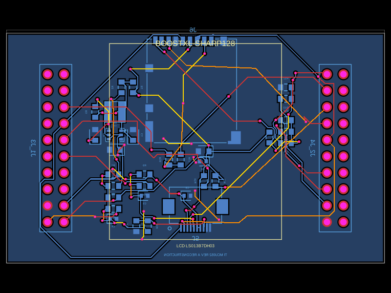 Similar packageabse/boostxl-sharp128This code defines a printed circuit board (PCB) with various surface-mount resistors, capacitors, inductors, and integrated circuits, including power management components and interface connectors, for a TI-based LCD and microSD module using 0603 and other package types.