tscircuit/boosters
This code defines PCB schematics, footprints, and 3D CAD models for various integrated circuits, connectors, sensors, and electronic components used in TI booster packs and modules.
- Version
- 0.1.19
- License
- unset
- Stars
- 0
boostxl-ads1119/imports/GPFA104_0202A003R1BA.tsx
import type { ChipProps } from "@tscircuit/props"

const pinLabels = {
  pin1: ["pin1"],
  pin2: ["pin2"]
} as const

export const GPFA104_0202A003R1BA = (props: ChipProps<typeof pinLabels>) => {
  return (
    <chip
      pinLabels={pinLabels}
      supplierPartNumbers={{
  "jlcpcb": [
    "C7434661"
  ]
}}
      manufacturerPartNumber="GPFA104_0202A003R1BA"
      footprint={<footprint>
        <platedhole  portHints={["pin2"]} pcbX="0.999998mm" pcbY="0mm" outerDiameter="1.3999972mm" holeDiameter="0.9000236mm" shape="circle" />
<platedhole  portHints={["pin1"]} pcbX="-0.999998mm" pcbY="0mm" outerDiameter="1.3999972mm" holeDiameter="0.9000236mm" shape="circle" />
<silkscreenpath route={[{"x":-1.9905979999999772,"y":1.0253979999999956},{"x":2.0159979999999678,"y":1.0253979999999956},{"x":2.0159979999999678,"y":-0.9999980000001187},{"x":-1.9905979999999772,"y":-0.9999980000001187},{"x":-1.9905979999999772,"y":1.0253979999999956}]} />
<silkscreenpath route={[{"x":1.1368683772161603e-13,"y":0.8890000000001237},{"x":1.1368683772161603e-13,"y":-0.88900000000001}]} />
<silkscreentext text="{NAME}" pcbX="-0.022098mm" pcbY="2.025398mm" anchorAlignment="center" fontSize="1mm" />
<courtyardoutline outline={[{"x":-2.2913979999999583,"y":1.2753979999999956},{"x":2.2472020000001294,"y":1.2753979999999956},{"x":2.2472020000001294,"y":-1.2820019999999204},{"x":-2.2913979999999583,"y":-1.2820019999999204},{"x":-2.2913979999999583,"y":1.2753979999999956}]} />
      </footprint>}
      cadModel={{
        objUrl: "https://modelcdn.tscircuit.com/easyeda_models/assets/C7434661.obj",
        stepUrl: "https://modelcdn.tscircuit.com/easyeda_models/assets/C7434661.step",
        pcbRotationOffset: 0,
        modelOriginPosition: { x: 0, y: -0.0050000000000000044, z: -0.0000055999999997169425 },
      }}
      {...props}
    />
  )
}
Related Packages
 More from this authortscircuit/autorouting-dataset-01This code manages the hardware and electronic components for circuit design and PCB layout, defining components like resistors, capacitors, transistors, connectors, and footprints, and providing tools for component placement, PCB topology, and electrical connections.
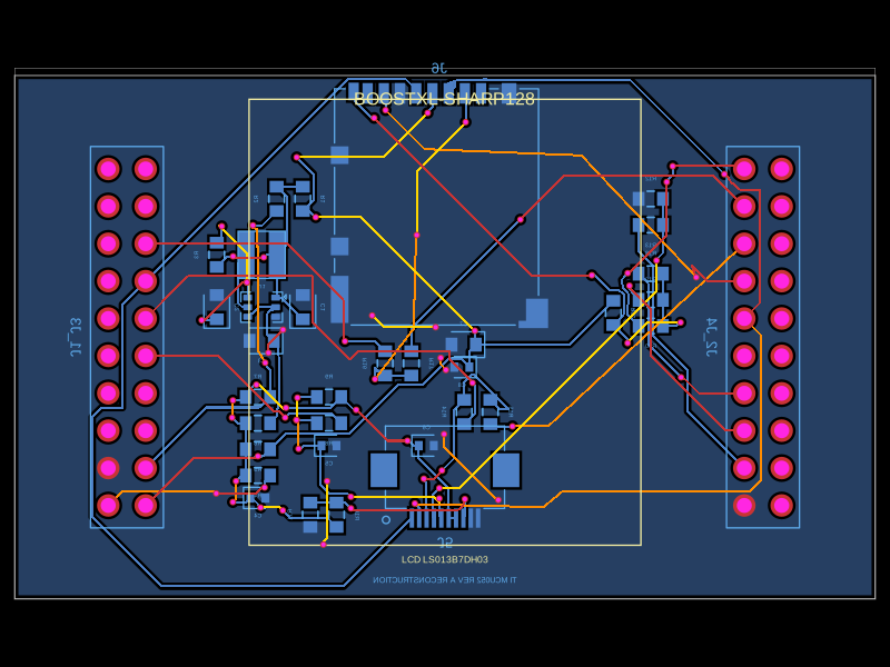 Similar packageabse/boostxl-sharp128This code defines a printed circuit board (PCB) with various surface-mount resistors, capacitors, inductors, and integrated circuits, including power management components and interface connectors, for a TI-based LCD and microSD module using 0603 and other package types.