techmannih/trellis-core
This code defines a detailed electronic hardware design incorporating various surface-mount components such as a crystal oscillator, crystal resonators, LEDs, connectors, ICs, inductors, resistors, capacitors, and a fuse, all arranged on a multi-layer PCB with specified footprints, schematic symbols, and 3D CAD models.
- Version
- 0.2.15
- License
- unset
- Stars
- 0
imports/XL_2121RGBC_2812B/XL_2121RGBC_2812B.tsx
import type { ChipProps } from "@tscircuit/props"

const pinLabels = {
  pin1: ["DIN"],
  pin2: ["VDD"],
  pin3: ["DO"],
  pin4: ["GND"]
} as const

const pinAttributes = {
  pin2: {requiresPower: true},
  pin4: {requiresGround: true}
} as const

export const XL_2121RGBC_2812B = (props: ChipProps<typeof pinLabels>) => {
  return (
    <chip
      pinLabels={pinLabels}
      pinAttributes={pinAttributes}
      supplierPartNumbers={{
  "jlcpcb": [
    "C5349957"
  ]
}}
      manufacturerPartNumber="XL-2121RGBC-2812B"
      footprint={<footprint>
        <smtpad portHints={["pin4"]} pcbX="-0.86995mm" pcbY="-0.499999mm" width="0.850011mm" height="0.5999988mm" shape="rect" />
<smtpad portHints={["pin3"]} pcbX="-0.86995mm" pcbY="0.499999mm" width="0.850011mm" height="0.5999988mm" shape="rect" />
<smtpad portHints={["pin2"]} pcbX="0.86995mm" pcbY="0.499999mm" width="0.850011mm" height="0.5999988mm" shape="rect" />
<smtpad portHints={["pin1"]} pcbX="0.86995mm" pcbY="-0.499999mm" width="0.850011mm" height="0.5999988mm" shape="rect" />
<silkscreenpath strokeWidth="0.15mm" route={[{"x":1.0500105999999505,"y":-1.0311891999999716},{"x":1.0500105999999505,"y":-1.0500359999999773}]} />
<silkscreenpath strokeWidth="0.15mm" route={[{"x":-1.0499597999998969,"y":1.0310622000000649},{"x":-1.0499597999998969,"y":1.0499344000000974},{"x":1.0500105999999505,"y":1.0499344000000974},{"x":1.0500105999999505,"y":1.0310622000000649}]} />
<silkscreenpath strokeWidth="0.15mm" route={[{"x":1.0500105999999505,"y":-1.0500359999999773},{"x":-1.0499597999998969,"y":-1.0500359999999773},{"x":-1.0499597999998969,"y":-1.0311891999999716}]} />
{/* PCB dot identifies pin 1 / DIN; see docs/assembly.md for the top-view map. */}
<silkscreencircle pcbX="1.7mm" pcbY="-1.05mm" radius="0.2mm" strokeWidth="0.18mm" />
<fabricationnotetext text="1 DIN" pcbX="1.8mm" pcbY="-2.0mm" fontSize="0.5mm" />
<fabricationnotepath route={[{ x: 1.8, y: -1.6 }, { x: 0.86995, y: -0.499999 }]}
  strokeWidth="0.15mm" />
<silkscreentext text="{NAME}" pcbX="0.1524mm" pcbY="2.0414mm" anchorAlignment="center" fontSize="1mm" />
<courtyardoutline outline={[{"x":-1.5453999999999724,"y":1.291400000000067},{"x":1.8502000000000862,"y":1.291400000000067},{"x":1.8502000000000862,"y":-1.3675999999999249},{"x":-1.5453999999999724,"y":-1.3675999999999249},{"x":-1.5453999999999724,"y":1.291400000000067}]} />
      </footprint>}

      {...props}
    />
  )
}
Related Packages
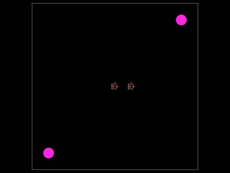 More from this authortechmannih/duplicate-NPTHA 50mm x 50mm PCB layout featuring two mounting holes, a 10kΩ resistor, and a 100nF capacitor positioned at specific coordinates.
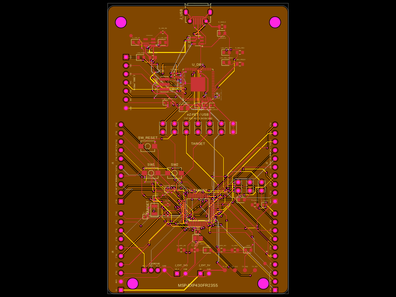 Similar packageShiboSoftwareDev/msp-exp430fr2355This code defines React components representing various surface-mount and through-hole electronic components—such as resonators, microcontrollers, crystals, connectors, and push buttons—with detailed physical footprints, 3D models, and pin configurations for PCB design.