pixalynx/pixal-gps
These files define two separate printed circuit boards: a small, two-layer battery cartridge with protection circuitry and contact pads for a pouch cell, and a larger, two-layer wireless charging dock featuring USB-C input, a resonant coil, and wireless power transmission components.
- Version
- 0.1.2
- License
- unset
- Stars
- 0
scripts/export-router-dsn.py
#!/usr/bin/env python3
"""Export a tscircuit build (circuit.json rendered with routingDisabled, i.e. lands + hand-planned copper only)
as a Specctra DSN for a local Freerouting pass.

- every land is its own single-pin component, so no footprint-frame or rotation assumptions leak into the exchange
- every pcb_trace / via already in the build (RF legs, ground mesh) is exported as fixed wiring
- inner1 is the unbroken GND plane (power layer: Freerouting never routes on it and, in practice, never drops plane vias either, so unresolved ground lands come back as surface links); top / inner2 / bottom are routing layers
- 0.4 mm edge keepouts on every routing layer; the 50-ohm RF lines get a wire keepout corridor on top and a via
  keepout on every layer so the reference plane under them stays solid
- nets: 0.15 mm signals, 0.20 mm power rails (widened to 0.30 afterwards where the DRC allows), 0.25 mm ground; 0.4/0.2 mm vias; 0.15 mm clearance

Usage: python3 scripts/export-router-dsn.py tracker
Writes tmp/router/<board>.dsn and tmp/router/<board>-pad-map.json (land -> pin id audit used by the importer).
"""
import json, sys, math, hashlib
board_key = sys.argv[1] if len(sys.argv) > 1 else 'tracker'
raw = open(f'dist/{board_key}/circuit.json', 'rb').read()
c = json.loads(raw)
POWER = {'VSYS', 'VBAT', 'VBUS_QI', 'VDD_NRF', 'RECT', 'VBUSOUT', 'AC1', 'AC2', 'COIL1'}
LAYERS = ['top', 'inner1', 'inner2', 'bottom']
ROUTING_LAYERS = ['top', 'inner2', 'bottom']
PLANE_LAYER = 'inner1'
EDGE = 0.4          # copper-to-edge keepout strip
RF_HALF = 0.5       # keepout half-width around 50-ohm lines (edge-to-edge gap >= 0.34 mm to a 0.15 mm trace)
um = lambda v: str(int(round(v * 1000)))

board = next(e for e in c if e['type'] == 'pcb_board')
bw, bh, bx, by = board['width'], board['height'], board['center']['x'], board['center']['y']
src_ports = {e['source_port_id']: e for e in c if e['type'] == 'source_port'}
src_comps = {e['source_component_id']: e['name'] for e in c if e['type'] == 'source_component'}
pcb_ports = {e['pcb_port_id']: e for e in c if e['type'] == 'pcb_port'}
nets_by_key = {}
for e in c:
    if e['type'] == 'source_net' and e.get('subcircuit_connectivity_map_key'):
        nets_by_key[e['subcircuit_connectivity_map_key']] = e['name']
def net_name(key):
    if not key: return None
    if key not in nets_by_key: nets_by_key[key] = 'N_' + key.rsplit('_', 1)[-1]
    return nets_by_key[key]
src_traces = {e['source_trace_id']: e for e in c if e['type'] == 'source_trace'}

lands = [e for e in c if e['type'] in ('pcb_smtpad', 'pcb_plated_hole')]
images, padstacks, placements, pins_by_net, pad_map = [], [], [], {}, []
for i, p in enumerate(lands):
    x, y = p['x'], p['y']
    if p['type'] == 'pcb_plated_hole':
        layers, shape = LAYERS, f"(circle %s {um(p['outer_diameter'])})"
        geo = {'shape': 'circle', 'd': p['outer_diameter']}
    elif p['shape'] == 'circle':
        layers, shape = [p['layer']], f"(circle %s {um(2 * p['radius'])})"
        geo = {'shape': 'circle', 'd': 2 * p['radius']}
    else:
        w, h, rot = p['width'], p['height'], math.radians(p.get('ccw_rotation') or 0)
        corners = [(-w / 2, -h / 2), (w / 2, -h / 2), (w / 2, h / 2), (-w / 2, h / 2)]
        pts = [(cx * math.cos(rot) - cy * math.sin(rot), cx * math.sin(rot) + cy * math.cos(rot)) for cx, cy in corners]
        layers, shape = [p['layer']], '(polygon %s 0 ' + ' '.join(f'{um(px)} {um(py)}' for px, py in pts) + ')'
        geo = {'shape': 'rect', 'w': w, 'h': h, 'rot': p.get('ccw_rotation') or 0}
    images.append(f'(image IMG{i} (pin PAD{i} 1 0 0))')
    padstacks.append(f'(padstack PAD{i} ' + ' '.join('(shape ' + shape % l + ')' for l in layers) + ' (attach off))')
    placements.append(f'(component IMG{i} (place P{i} {um(x)} {um(y)} front 0))')
    port = pcb_ports.get(p.get('pcb_port_id'))
    sp = src_ports.get(port['source_port_id']) if port else None
    net = net_name(sp.get('subcircuit_connectivity_map_key')) if sp else None
    if net: pins_by_net.setdefault(net, []).append(f'P{i}-1')
    pad_map.append({'pin': f'P{i}', 'land': p.get('pcb_smtpad_id') or p.get('pcb_plated_hole_id'), 'port': p.get('pcb_port_id'),
                    'ref': (src_comps.get(sp['source_component_id']) + '.' + (sp.get('name') or sp['source_port_id'])) if sp else None,
                    'net': net, 'x': x, 'y': y, 'layers': layers, 'geo': geo})

# fixed copper already in the build
wires, fixed_vias, rf_segments = [], [], []
for t in c:
    if t['type'] != 'pcb_trace': continue
    st = src_traces.get(t.get('source_trace_id'))
    net = net_name(st.get('subcircuit_connectivity_map_key')) if st else None
    if not net: raise SystemExit(f"fixed trace {t['pcb_trace_id']} has no net")
    poly, layer, width = [], None, None
    is_rf = (st.get('name') or '').startswith('rf_')
    def flush():
        if len(poly) >= 2:
            wires.append(f'(wire (path {layer} {um(width)} ' + ' '.join(f'{um(px)} {um(py)}' for px, py in poly) + f') (net {net}) (type fix))')
            if is_rf and layer == 'top': rf_segments.extend(zip(poly, poly[1:]))
    for pt in t['route']:
        if pt['route_type'] == 'via':
            flush(); poly = []
            fixed_vias.append(f"(via VIA400_200 {um(pt['x'])} {um(pt['y'])} (net {net}) (type fix))")
            continue
        if pt['layer'] != layer or (width is not None and abs(pt['width'] - width) > 1e-6):
            flush(); poly = [poly[-1]] if poly and pt['layer'] == layer else []
            layer, width = pt['layer'], pt['width']
        poly.append((pt['x'], pt['y']))
    flush()

# keepouts: board edge strips and RF corridors
x0, y0, x1, y1 = bx - bw / 2, by - bh / 2, bx + bw / 2, by + bh / 2
keepouts = []
for l in ROUTING_LAYERS:
    for rx0, ry0, rx1, ry1 in [(x0, y0, x1, y0 + EDGE), (x0, y1 - EDGE, x1, y1), (x0, y0, x0 + EDGE, y1), (x1 - EDGE, y0, x1, y1)]:
        keepouts.append(f'(keepout (rect {l} {um(rx0)} {um(ry0)} {um(rx1)} {um(ry1)}))')
for h in (e for e in c if e['type'] == 'pcb_hole'):
    d = (h.get('hole_diameter') or max(h.get('hole_width', 0), h.get('hole_height', 0))) + 1.0
    for l in ROUTING_LAYERS: keepouts.append(f"(keepout (circle {l} {um(d)} {um(h['x'])} {um(h['y'])}))")
for (ax, ay), (bx_, by_) in rf_segments:
    dx, dy = bx_ - ax, by_ - ay
    n = math.hypot(dx, dy) or 1
    ux, uy, nx, ny = dx / n, dy / n, -dy / n, dx / n
    ex = 0.2
    pts = [(ax - ux * ex + nx * RF_HALF, ay - uy * ex + ny * RF_HALF), (bx_ + ux * ex + nx * RF_HALF, by_ + uy * ex + ny * RF_HALF),
           (bx_ + ux * ex - nx * RF_HALF, by_ + uy * ex - ny * RF_HALF), (ax - ux * ex - nx * RF_HALF, ay - uy * ex - ny * RF_HALF)]
    poly = ' '.join(f'{um(px)} {um(py)}' for px, py in pts)
    keepouts.append(f'(keepout (polygon top 0 {poly}))')
    for l in ROUTING_LAYERS: keepouts.append(f'(via_keepout (polygon {l} 0 {poly}))')

gnd = nets_by_key.get(next(e['subcircuit_connectivity_map_key'] for e in c if e['type'] == 'source_net' and e['name'] == 'GND'))
plane = f'(plane {gnd} (polygon {PLANE_LAYER} 0 {um(x0 + EDGE)} {um(y0 + EDGE)} {um(x1 - EDGE)} {um(y0 + EDGE)} {um(x1 - EDGE)} {um(y1 - EDGE)} {um(x0 + EDGE)} {um(y1 - EDGE)}))'
net_names = sorted(pins_by_net)
classes = [
    f"(class POWER {' '.join(n for n in net_names if n in POWER)} (circuit (use_via VIA400_200)) (rule (width 200) (clearance 120)))",
    f"(class GROUND {gnd} (circuit (use_via VIA400_200)) (rule (width 250) (clearance 120)))",
    f"(class SIGNAL {' '.join(n for n in net_names if n not in POWER and n != gnd)} (circuit (use_via VIA400_200)) (rule (width 150) (clearance 120)))",
]
padstacks.append('(padstack VIA400_200 ' + ' '.join(f'(shape (circle {l} 400))' for l in LAYERS) + ' (attach off))')
dsn = f"""(pcb {board_key}
 (parser (string_quote ") (space_in_quoted_tokens on) (host_cad "tscircuit") (host_version "pixal-gps"))
 (resolution um 10) (unit um)
 (structure
  {chr(10).join(f'(layer {l} (type {"power" if l == PLANE_LAYER else "signal"}) (property (index {i})))' for i, l in enumerate(LAYERS))}
  (boundary (path pcb 0 {um(x0)} {um(y0)} {um(x1)} {um(y0)} {um(x1)} {um(y1)} {um(x0)} {um(y1)} {um(x0)} {um(y0)}))
  {plane}
  {chr(10).join(keepouts)}
  (via VIA400_200)
  (rule (width 150) (clearance 120) (clearance 50 (type smd_smd)))
 )
 (placement {chr(10).join(placements)})
 (library {chr(10).join(images)} {chr(10).join(padstacks)})
 (network
  {chr(10).join(f'(net {n} (pins {" ".join(pins_by_net[n])}))' for n in net_names)}
  {chr(10).join(classes)}
 )
 (wiring
  {chr(10).join(wires)}
  {chr(10).join(fixed_vias)}
 )
)
"""
open(f'tmp/router/{board_key}.dsn', 'w').write(dsn)
json.dump({'source_sha256': hashlib.sha256(raw).hexdigest(), 'lands': pad_map}, open(f'tmp/router/{board_key}-pad-map.json', 'w'), indent=1)
print(f'{board_key}: {len(lands)} lands, {len(net_names)} nets, {len(wires)} fixed wires, {len(fixed_vias)} fixed vias, {len(rf_segments)} RF segments, {len(keepouts)} keepouts')
Related Packages
 More from this authorpixalynx/esp32-gps-cellular-trackerThis code defines a hardware layout comprising a Wi-Fi-enabled ESP32 module, GPS module, cellular GSM module, battery management components (including charger, protection circuits, and voltage regulators), USB-C connector, SIM card holder, RF components, and supporting passive components for a comprehensive GPS+Cellular tracker device.
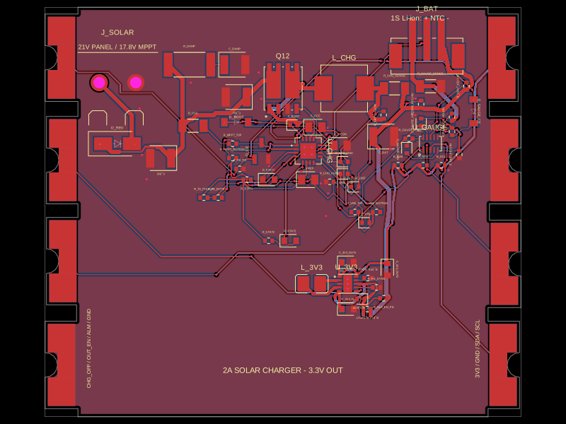 Similar packageShiboSoftwareDev/solar-battery-charger-moduleThis hardware setup integrates a solar panel, a lithium-ion battery, and a multi-rail buck converter with a battery charging IC, protection circuitry, and monitoring components, enabling solar power harvesting, battery charging, and power distribution in an embedded system.
 Discover something newimrishabh18/fitness_watchThis circuit integrates an ESP-12E microcontroller with various sensors and peripherals, including a AO3400A MOSFET for switching loads, to enable wireless control and sensor data processing.