pixalynx/pixal-gps
These files define two separate printed circuit boards: a small, two-layer battery cartridge with protection circuitry and contact pads for a pouch cell, and a larger, two-layer wireless charging dock featuring USB-C input, a resonant coil, and wireless power transmission components.
- Version
- 0.1.2
- License
- unset
- Stars
- 0
review/source-build/scripts/gen-gnd-mesh.py
#!/usr/bin/env python3
"""Generate routing/gnd-mesh.json for a board: for every land on the ground net, either a short
stub to a new plane via (preferred) or a straight same-layer link to the nearest other ground
land whose path is clear. Lands that get neither are listed so they can be handled by hand.

Usage: gen-gnd-mesh.py dist/<board>/circuit.json routing/<board>-gnd.json [NET]
Via: 0.4 mm land / 0.2 mm drill, >= 0.18 mm from any other land or hole on any layer and from
the board edge; link: 0.2 mm wide, >= 0.15 mm from every other land on its layer.
"""
import json, sys, math
src, out = sys.argv[1], sys.argv[2]; NET = sys.argv[3] if len(sys.argv) > 3 else 'GND'
VIA_D, CLEAR, STEP, LINK_W, LINK_MAX = 0.4, 0.18, 0.45, 0.2, 3.0
d = json.load(open(src))
board = next(e for e in d if e['type'] == 'pcb_board'); bw, bh = board['width'], board['height']; bx, by = board['center']['x'], board['center']['y']
comps = {c['pcb_component_id']: c for c in d if c['type'] == 'pcb_component'}
sname = {c['source_component_id']: c['name'] for c in d if c['type'] == 'source_component'}
sports = {p['source_port_id']: p for p in d if p['type'] == 'source_port'}
nets = {n['source_net_id']: n for n in d if n['type'] == 'source_net'}
gnd_ids = [nid for nid, n in nets.items() if n['name'] == NET]
gnd_key = None
for t in d:
    if t['type'] == 'source_trace' and any(n in t.get('connected_source_net_ids', []) for n in gnd_ids):
        for pid in t.get('connected_source_port_ids', []): gnd_key = sports[pid].get('subcircuit_connectivity_map_key'); break
    if gnd_key: break
gnd_ports = {pid for pid, p in sports.items() if p.get('subcircuit_connectivity_map_key') == gnd_key}
elems = [e for e in d if e['type'] in ('pcb_smtpad', 'pcb_plated_hole', 'pcb_hole')]
def rect(e):
    if e['type'] == 'pcb_smtpad':
        if e['shape'] == 'circle': r = e['radius']; return (e['x'] - r, e['y'] - r, e['x'] + r, e['y'] + r)
        return (e['x'] - e['width'] / 2, e['y'] - e['height'] / 2, e['x'] + e['width'] / 2, e['y'] + e['height'] / 2)
    r = (e.get('outer_diameter') or e.get('hole_diameter') or e.get('diameter')) / 2
    return (e['x'] - r, e['y'] - r, e['x'] + r, e['y'] + r)
def rdist(x, y, r):
    x0, y0, x1, y1 = r; return math.hypot(max(x0 - x, 0, x - x1), max(y0 - y, 0, y - y1))
def seg_rect_dist(ax, ay, bx_, by_, r):
    # distance from segment AB to rectangle r (sampled)
    n = 12; best = 1e9
    for i in range(n + 1):
        t = i / n; best = min(best, rdist(ax + (bx_ - ax) * t, ay + (by_ - ay) * t, r))
    return best
rects = [(rect(e), e) for e in elems]
# escape lanes: the 0.6 mm strip outward of every land of a multi-pin part (chips, connectors) stays free of other
# parts' stub vias/links so the signal router can leave those lands (a stub via there blocked U5.FOD, U3.SCL ...)
ESCAPE = 0.6
pads_by_comp = {}
for e in elems:
    if e['type'] == 'pcb_smtpad' and e.get('pcb_component_id'): pads_by_comp.setdefault(e['pcb_component_id'], []).append(e)
escape_rects = []  # (rect, component id, layer)
for cid, pads in pads_by_comp.items():
    if len(pads) < 6: continue
    cx, cy = comps[cid]['center']['x'], comps[cid]['center']['y']
    hw = max(abs(p['x'] - cx) for p in pads) or 1; hh = max(abs(p['y'] - cy) for p in pads) or 1
    for p in pads:
        if p['shape'] == 'circle': continue
        x0, y0, x1, y1 = rect(p); ndx, ndy = (p['x'] - cx) / hw, (p['y'] - cy) / hh
        if abs(ndx) >= abs(ndy): r = (x1, y0 - 0.05, x1 + ESCAPE, y1 + 0.05) if ndx > 0 else (x0 - ESCAPE, y0 - 0.05, x0, y1 + 0.05)
        else: r = (x0 - 0.05, y1, x1 + 0.05, y1 + ESCAPE) if ndy > 0 else (x0 - 0.05, y0 - ESCAPE, x1 + 0.05, y0)
        escape_rects.append((r, cid, p['layer']))
# hand-routed copper present in this build (RF lines): keep vias off it
segs = []
for tr in d:
    if tr['type'] != 'pcb_trace': continue
    pts = [(p['x'], p['y'], p.get('width', 0.15), p.get('layer')) for p in tr['route'] if p.get('route_type') == 'wire']
    if not pts: continue  # all hand-routed copper in the placement build (RF lines, hand legs); the mesh itself is empty at this point
    for a, b in zip(pts, pts[1:]): segs.append((a[0], a[1], b[0], b[1], max(a[2], b[2]), a[3]))
def seg_pt_dist(x, y, ax, ay, bx_, by_):
    dx, dy = bx_ - ax, by_ - ay; l2 = dx * dx + dy * dy
    t_ = 0 if l2 == 0 else max(0, min(1, ((x - ax) * dx + (y - ay) * dy) / l2))
    return math.hypot(x - (ax + t_ * dx), y - (ay + t_ * dy))
def sel_of(pp):
    sp = sports[pp['source_port_id']]; name = sname[comps[[e for e in elems if e.get('pcb_port_id') == pp['pcb_port_id']][0]['pcb_component_id']]['source_component_id']]
    pn = sp.get('name') or ''; hints = pp.get('port_hints', [])
    pin_hint = next((h for h in hints if h.startswith('pin')), None) or next((f"pin{h}" for h in hints if h.isdigit()), None)
    return f"{name}.{pn}" if pn and not pn.startswith('pin') else f"{name}.{pin_hint or pn}"
gnd_pads = []
for pp in [p for p in d if p['type'] == 'pcb_port' and p.get('source_port_id') in gnd_ports]:
    pad = next((e for e in elems if e['type'] == 'pcb_smtpad' and e.get('pcb_port_id') == pp['pcb_port_id']), None)
    if pad: gnd_pads.append((sel_of(pp), pad))
gnd_pad_ids = {id(p) for _, p in gnd_pads}
stubs, links, taken, todo = [], [], [(v['x'], v['y']) for v in d if v['type'] == 'pcb_via'], []  # existing vias (hand legs) are taken spots
for sel, pad in gnd_pads:
    comp = comps[pad['pcb_component_id']]
    w, h = (pad['radius'] * 2, pad['radius'] * 2) if pad['shape'] == 'circle' else (pad['width'], pad['height'])
    dx, dy = pad['x'] - comp['center']['x'], pad['y'] - comp['center']['y']
    sx, sy = math.copysign(1, dx or 1), math.copysign(1, dy or 1)
    cands = [(sx, 0), (0, sy), (0, -sy), (-sx, 0), (0.7071 * sx, 0.7071), (0.7071 * sx, -0.7071)] if abs(dx) >= abs(dy) else [(0, sy), (sx, 0), (-sx, 0), (0, -sy), (0.7071, 0.7071 * sy), (-0.7071, 0.7071 * sy)]
    placed = None
    for ux, uy in cands:
        for extra in (0, 0.15, 0.3, 0.45):
            x = pad['x'] + ux * (w / 2 + STEP + extra); y = pad['y'] + uy * (h / 2 + STEP + extra)
            if abs(x - bx) > bw / 2 - 0.55 or abs(y - by) > bh / 2 - 0.55: continue  # 0.2 via radius + 0.3 edge clearance
            if any(rdist(x, y, r) < VIA_D / 2 + CLEAR for r, e in rects if e is not pad): continue
            if any(math.hypot(tx - x, ty - y) < VIA_D + CLEAR for tx, ty in taken): continue
            if any(rdist(x, y, r) < VIA_D / 2 + 0.15 for r, cid, _ in escape_rects if cid != pad['pcb_component_id']): continue
            if any(seg_rect_dist(pad['x'], pad['y'], x, y, r) < LINK_W / 2 + 0.15 for r, cid, l in escape_rects if cid != pad['pcb_component_id'] and l == pad['layer']): continue
            if any(seg_pt_dist(x, y, *s[:4]) < VIA_D / 2 + s[4] / 2 + 0.2 for s in segs): continue
            # the stub segment from the pad centre to the via must not touch other lands on the pad's layer
            if any(seg_rect_dist(pad['x'], pad['y'], x, y, r) < LINK_W / 2 + 0.15 for r, e in rects if e is not pad and e['type'] == 'pcb_smtpad' and e.get('layer') == pad['layer']): continue
            placed = (round(x, 3), round(y, 3)); break
        if placed: break
    if placed:
        taken.append(placed)
        rot = math.radians(comp.get('rotation') or 0)
        vx, vy = placed[0] - comp['center']['x'], placed[1] - comp['center']['y']
        lx, ly = vx * math.cos(-rot) - vy * math.sin(-rot), vx * math.sin(-rot) + vy * math.cos(-rot)
        # core applies only translate+rotate to pcbPath points (no bottom mirror), so no x flip here
        stubs.append({"port": sel, "layer": pad['layer'], "pad": [round(pad['x'], 3), round(pad['y'], 3)], "via": list(placed), "local": [round(lx, 3), round(ly, 3)]})
    else:
        todo.append((sel, pad))
# second pass: link leftover pads to the nearest ground land on the same layer with a clear straight path
final_todo = []
for sel, pad in todo:
    best = None
    resolved = {s['port'] for s in stubs}
    for sel2, pad2 in gnd_pads:
        if pad2 is pad or pad2['layer'] != pad['layer'] or sel2 not in resolved: continue
        dist = math.hypot(pad2['x'] - pad['x'], pad2['y'] - pad['y'])
        if dist > LINK_MAX or (best and dist >= best[0]): continue
        blocked = any(seg_rect_dist(pad['x'], pad['y'], pad2['x'], pad2['y'], r) < LINK_W / 2 + 0.15 for r, e in rects if e is not pad and e is not pad2 and e['type'] == 'pcb_smtpad' and e.get('layer') == pad['layer'])
        if not blocked and any(seg_rect_dist(pad['x'], pad['y'], pad2['x'], pad2['y'], r) < LINK_W / 2 + 0.15 for r, cid, l in escape_rects if cid not in (pad['pcb_component_id'], pad2['pcb_component_id']) and l == pad['layer']): blocked = True
        if not blocked: best = (dist, sel2, pad2)
    if best: links.append({"from": sel, "to": best[1], "layer": pad['layer'], "a": [round(pad['x'], 3), round(pad['y'], 3)], "b": [round(best[2]['x'], 3), round(best[2]['y'], 3)]})
    else: final_todo.append(sel)
json.dump({"stubs": stubs, "links": links, "unresolved": final_todo}, open(out, 'w'), indent=1)
print(f"{len(gnd_pads)} ground lands: {len(stubs)} via stubs, {len(links)} links, unresolved {final_todo}")
Related Packages
 More from this authorpixalynx/esp32-gps-cellular-trackerThis code defines a hardware layout comprising a Wi-Fi-enabled ESP32 module, GPS module, cellular GSM module, battery management components (including charger, protection circuits, and voltage regulators), USB-C connector, SIM card holder, RF components, and supporting passive components for a comprehensive GPS+Cellular tracker device.
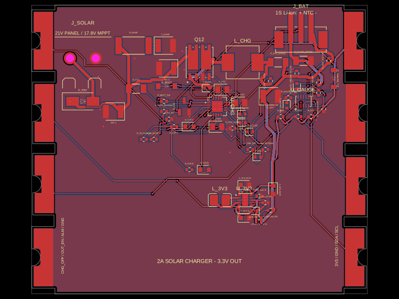 Similar packageShiboSoftwareDev/solar-battery-charger-moduleThis hardware setup integrates a solar panel, a lithium-ion battery, and a multi-rail buck converter with a battery charging IC, protection circuitry, and monitoring components, enabling solar power harvesting, battery charging, and power distribution in an embedded system.
 Discover something newimrishabh18/fitness_watchThis circuit integrates an ESP-12E microcontroller with various sensors and peripherals, including a AO3400A MOSFET for switching loads, to enable wireless control and sensor data processing.