pixalynx/pixal-gps
These files define two separate printed circuit boards: a small, two-layer battery cartridge with protection circuitry and contact pads for a pouch cell, and a larger, two-layer wireless charging dock featuring USB-C input, a resonant coil, and wireless power transmission components.
- Version
- 0.1.2
- License
- unset
- Stars
- 0
review/source-build/scripts/check-clearance.py
#!/usr/bin/env python3
"""Independent copper clearance audit for a built board (tscircuit's checker does not flag every trace-to-pad case).
Reports, per layer: trace/via copper closer than MIN to a land, via or trace of a different net, and copper closer
than EDGE to the board outline. Usage: python3 scripts/check-clearance.py dist/tracker/circuit.json [--json out]
"""
import json, sys, math
MIN, EDGE = 0.10, 0.30
path = sys.argv[1]
c = json.load(open(path))
board = next(e for e in c if e['type'] == 'pcb_board')
bx0, by0 = board['center']['x'] - board['width'] / 2, board['center']['y'] - board['height'] / 2
bx1, by1 = board['center']['x'] + board['width'] / 2, board['center']['y'] + board['height'] / 2
LAYERS = ['top', 'inner1', 'inner2', 'bottom']
ports = {p['pcb_port_id']: p for p in c if p['type'] == 'pcb_port'}
sports = {p['source_port_id']: p for p in c if p['type'] == 'source_port'}
sc = {e['source_component_id']: e['name'] for e in c if e['type'] == 'source_component'}
st = {e['source_trace_id']: e for e in c if e['type'] == 'source_trace'}
def port_net(pid):
    p = ports.get(pid); sp = sports.get(p['source_port_id']) if p else None
    return sp.get('subcircuit_connectivity_map_key') if sp else None
def port_name(pid):
    p = ports.get(pid); sp = sports.get(p['source_port_id']) if p else None
    return f"{sc.get(sp['source_component_id'])}.{sp.get('name')}" if sp else pid
# lands: (layer set, geometry, net, name)
lands = []
for e in c:
    if e['type'] == 'pcb_smtpad':
        g = ('circle', e['x'], e['y'], e['radius']) if e['shape'] == 'circle' else ('rect', e['x'], e['y'], e['width'], e['height'], e.get('ccw_rotation') or 0)
        lands.append(({e['layer']}, g, port_net(e.get('pcb_port_id')), port_name(e.get('pcb_port_id'))))
    elif e['type'] == 'pcb_plated_hole':
        if e.get('outer_diameter'): g = ('circle', e['x'], e['y'], e['outer_diameter'] / 2)
        else: g = ('rect', e['x'], e['y'], e.get('outer_width') or e.get('hole_width'), e.get('outer_height') or e.get('hole_height'), e.get('ccw_rotation') or 0)
        lands.append((set(LAYERS), g, port_net(e.get('pcb_port_id')), port_name(e.get('pcb_port_id'))))
    elif e['type'] == 'pcb_hole':
        d = e.get('hole_diameter') or max(e.get('hole_width', 0), e.get('hole_height', 0))
        lands.append((set(LAYERS), ('circle', e['x'], e['y'], d / 2), 'HOLE', 'hole'))
def pt_land(px, py, g):
    if g[0] == 'circle': return max(0.0, math.hypot(px - g[1], py - g[2]) - g[3])
    _, x, y, w, h, rot = g; r = -math.radians(rot); dx, dy = px - x, py - y
    rx, ry = dx * math.cos(r) - dy * math.sin(r), dx * math.sin(r) + dy * math.cos(r)
    return math.hypot(max(abs(rx) - w / 2, 0), max(abs(ry) - h / 2, 0))
def seg_land(a, b, g, n=10):
    return min(pt_land(a[0] + (b[0] - a[0]) * i / n, a[1] + (b[1] - a[1]) * i / n, g) for i in range(n + 1))
def seg_seg(a, b, u, v):
    def sp(p, a, b):
        vx, vy = b[0] - a[0], b[1] - a[1]; l2 = vx * vx + vy * vy
        t = 0 if l2 == 0 else max(0, min(1, ((p[0] - a[0]) * vx + (p[1] - a[1]) * vy) / l2))
        return math.hypot(p[0] - a[0] - t * vx, p[1] - a[1] - t * vy)
    def cross(o, a, b): return (a[0] - o[0]) * (b[1] - o[1]) - (a[1] - o[1]) * (b[0] - o[0])
    d1, d2, d3, d4 = cross(u, v, a), cross(u, v, b), cross(a, b, u), cross(a, b, v)
    if ((d1 > 0) != (d2 > 0)) and ((d3 > 0) != (d4 > 0)) and d1 != 0 and d2 != 0: return 0.0
    return min(sp(a, u, v), sp(b, u, v), sp(u, a, b), sp(v, a, b))
segs, vias = [], []
for t in c:
    if t['type'] != 'pcb_trace': continue
    s = st.get(t.get('source_trace_id'), {}); net = s.get('subcircuit_connectivity_map_key'); name = s.get('name') or t['pcb_trace_id']
    prev = None
    for p in t['route']:
        if p['route_type'] == 'via': vias.append((p['x'], p['y'], p.get('via_diameter') or 0.4, net, name)); prev = None; continue
        if prev and prev['layer'] == p['layer']: segs.append((p['layer'], (prev['x'], prev['y']), (p['x'], p['y']), p.get('width', 0.15), net, name))
        prev = p
for v in c:
    if v['type'] == 'pcb_via':
        if not any(abs(v['x'] - x) < 1e-6 and abs(v['y'] - y) < 1e-6 for x, y, *_ in vias): vias.append((v['x'], v['y'], v.get('outer_diameter') or 0.4, None, v['pcb_via_id']))
viol = []
for layer, a, b, w, net, name in segs:
    for ls, g, lnet, lname in lands:
        if layer not in ls or (net and lnet and net == lnet): continue
        d = seg_land(a, b, g) - w / 2
        if d < MIN - 1e-6: viol.append((round(d, 3), layer, 'trace-land', name, lname))
    for x, y, dia, vnet, vname in vias:
        if net and vnet and net == vnet: continue
        d = seg_seg(a, b, (x, y), (x, y)) - w / 2 - dia / 2
        if d < MIN - 1e-6: viol.append((round(d, 3), layer, 'trace-via', name, vname))
    e = min(a[0] - bx0, bx1 - a[0], a[1] - by0, by1 - a[1], b[0] - bx0, bx1 - b[0], b[1] - by0, by1 - b[1]) - w / 2
    if e < EDGE - 1e-6: viol.append((round(e, 3), layer, 'trace-edge', name, 'board edge'))
for i, (layer, a, b, w, net, name) in enumerate(segs):
    for layer2, u, v, w2, net2, name2 in segs[i + 1:]:
        if layer != layer2 or (net and net2 and net == net2) or name == name2: continue
        if max(abs(a[0] - u[0]), abs(a[1] - u[1])) > 6: continue
        d = seg_seg(a, b, u, v) - w / 2 - w2 / 2
        if d < MIN - 1e-6: viol.append((round(d, 3), layer, 'trace-trace', name, name2))
for x, y, dia, vnet, vname in vias:
    for ls, g, lnet, lname in lands:
        if vnet and lnet and vnet == lnet: continue
        d = pt_land(x, y, g) - dia / 2
        if d < MIN - 1e-6: viol.append((round(d, 3), 'all', 'via-land', vname, lname))
    e = min(x - bx0, bx1 - x, y - by0, by1 - y) - dia / 2
    if e < EDGE - 1e-6: viol.append((round(e, 3), 'all', 'via-edge', vname, 'board edge'))
for i, (x, y, dia, vnet, vname) in enumerate(vias):
    for x2, y2, dia2, vnet2, vname2 in vias[i + 1:]:
        if vnet and vnet2 and vnet == vnet2: continue
        d = math.hypot(x - x2, y - y2) - dia / 2 - dia2 / 2
        if d < MIN - 1e-6: viol.append((round(d, 3), 'all', 'via-via', vname, vname2))
viol.sort()
print(f"{len(segs)} segments, {len(vias)} vias, {len(lands)} lands; {len(viol)} clearance findings below {MIN} mm (edge {EDGE} mm)")
for v in viol[:40]: print('  ', v)
if '--json' in sys.argv: json.dump(viol, open(sys.argv[sys.argv.index('--json') + 1], 'w'), indent=1)
sys.exit(1 if viol else 0)
Related Packages
 More from this authorpixalynx/esp32-gps-cellular-trackerThis code defines a hardware layout comprising a Wi-Fi-enabled ESP32 module, GPS module, cellular GSM module, battery management components (including charger, protection circuits, and voltage regulators), USB-C connector, SIM card holder, RF components, and supporting passive components for a comprehensive GPS+Cellular tracker device.
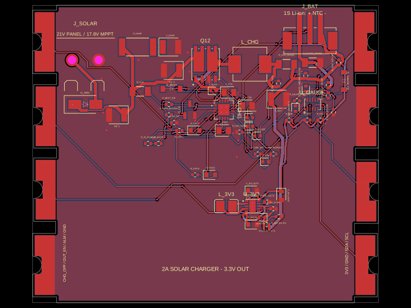 Similar packageShiboSoftwareDev/solar-battery-charger-moduleThis hardware setup integrates a solar panel, a lithium-ion battery, and a multi-rail buck converter with a battery charging IC, protection circuitry, and monitoring components, enabling solar power harvesting, battery charging, and power distribution in an embedded system.
 Discover something newimrishabh18/fitness_watchThis circuit integrates an ESP-12E microcontroller with various sensors and peripherals, including a AO3400A MOSFET for switching loads, to enable wireless control and sensor data processing.