pixalynx/pixal-gps
These files define two separate printed circuit boards: a small, two-layer battery cartridge with protection circuitry and contact pads for a pouch cell, and a larger, two-layer wireless charging dock featuring USB-C input, a resonant coil, and wireless power transmission components.
- Version
- 0.1.2
- License
- unset
- Stars
- 0
review/FAB-READINESS.md
# PIXAL GPS Rev A — fabrication readiness review

Reviewed 15 September 2026 (Australia/Sydney). **Not ready to order as a working three-board product.** Both the tracker and the battery interface contain release-blocking connectivity issues. The dock has no tscircuit error records in the available export, but an independent check finds two via-clearance violations at its declared 0.15 mm rule; its power routing and manufacturing preparation also need sign-off.

This is an inspection report, not an implementation. Original circuit sources, part definitions, route files and board exports were preserved. The new product viewer is a mechanical concept, not manufacturing CAD.

## 1. Tracker: five unrouted signal/power pads — blocker

`bun run check` fails with six missing endpoint records. A fresh tracker build in `review/source-build` reproduces the same failure, so this is not merely an old status paragraph. Inspection of the exported pad/trace geometry finds no trace reaching these five non-ground pads:

| Pad | Net | Consequence |
| --- | --- | --- |
| U3.VBUS | VBUS_QI | Qi output does not reach the PMIC input at this land; normal wireless battery charging cannot work. |
| U6.SCL | I2C_SCL | Accelerometer clock input is disconnected. |
| U6.INT1 | ACC_INT1 | Accelerometer interrupt output is disconnected. |
| U1.P0_31 | ACC_INT1 | The modem/application processor cannot receive the intended motion interrupt. |
| R13.pin1 | QI_FOD | The intended FOD/current-limit resistor network is incomplete. |

The checker also flags **C41.pin2**, but that pad lies inside the bottom GND pour (`pcb_copper_pour_55`, containing many vias). It should not be called a confirmed open simply because it lacks a trace-end ID. Its plane connectivity needs to be accepted by a geometry-aware connectivity check. The other five pads are not covered by a pour and their nearest trace geometry does not reach them.

**Outstanding:** complete these connections, then verify every net as connected copper after export, including branches, pours and vias. Re-run the existing assertions and an independent connectivity/DRC check. Source declarations alone are insufficient when `routingDisabled` is used.

References: [tracker source](../tracker.circuit.tsx), [route import](../routing/tracker-routes.json), [original validation failure](evidence/validate.txt), [fresh-build failure](evidence/fresh-validate.txt), [geometry metrics](evidence/design-metrics.json).

## 2. Battery PCB: NTC and bypass return are not GND — blocker

The tracker assertion stops the normal validator before it evaluates the battery PCB. A separate review-only harness collected failures without stopping at the first one. It uncovered two more failed assertions: `NTC to GND` and `JP1 bridges the FET pair only when fitted`.

In the battery export, **R3.pin2 and JP1.pin2 share connectivity net11**, while **P2, Q1.S2 and R4.pin2 are on net2 (GND)**. The explicit leg connects R3.pin2 to JP1.pin2 but does not declare their connection to GND. The ground-pour declaration does not repair the intended source-net connection.

This leaves the NTC return outside the intended ground network. The PMIC cannot rely on the intended 10 kΩ battery-temperature reading. The alternate PCM-cell assembly configuration also lacks the intended JP1 bridge from CELL_N to GND. The populated BQ29700/FS8205A protection path is a separate path; this finding does not imply that it has been bypassed in the default assembly.

**Outstanding:** resolve the NTC/JP1 ground connection and check both mutually exclusive battery-protection population variants. Confirm the selected cell is bare or PCM protected and issue the matching assembly BOM. Confirm the thermistor's physical thermal contact with the cell.

References: [battery circuit](../battery-pack.circuit.tsx), [all assertions](evidence/all-assertions.txt). The review harness says “evaluated”; 342 checks were evaluated and three failed, including the tracker coverage check.

## 3. Dock clearances and power copper — pre-order engineering review

A review-only run of the clearance checker at the dock's declared **0.15 mm** minimum reports two different-net via-to-via gaps: **0.100 mm** (`source_trace_34_0` / `source_trace_32_0`) and **0.123 mm** (`source_net_16_mst1_0` / `source_trace_34_0`). Resolve these against the agreed fabrication rules. The pack passes this stricter check. See [dock 0.15 mm evidence](evidence/dock-clearance-015.txt).

The dock declares VIN at 0.8 mm and PGND/LX1/LX2/COIL_A at 1.0 mm nominal widths. Its actual routed copper is much narrower:

| Dock net | Exported trace widths |
| --- | --- |
| VIN, PGND | 0.15–0.25 mm |
| LX1 | 0.20–0.25 mm |
| LX2 | 0.15–0.20 mm |
| COIL_A | 0.25 mm |

These are not just schematic labels. For example, the exported LX2 route has approximately 33.6 mm of centerline segments. This needs resistance, temperature-rise and resonant-current analysis; a 5 W input rating does not specify the circulating RMS coil current. Confirm the sense resistor's connections are genuinely Kelvin connections in the layout and do not share an appreciable power-current path.

The tracker also retains 0.20 mm sections on VBAT, VSYS, VBUS_QI and the AC nets, including inner-layer routing. No current/voltage-drop validation is present in the checks. This is a required engineering gate, not a claim that every narrow segment inevitably fails.

For the receiver, TI calls for low-resistance AC paths, close RECT/OUT bypassing and short ILIM/FOD loops. The project's own notes acknowledge the remote RECT capacitors. For example, C41's RECT land is roughly 7.5 mm in a straight line from U5.RECT, before accounting for its routed path. Resolve the return-path and high-frequency layout before release, and validate at intended current. [TI BQ51013B datasheet, §11](https://www.ti.com/lit/ds/symlink/bq51013b.pdf).

References: [dock source](../dock.circuit.tsx), [measured net widths](evidence/design-metrics.json), [wireless charging notes](../docs/wireless-charging.md). Summed trace lengths in the metrics are not automatically end-to-end lengths; the tracker importer can repeat shared trunks.

## 4. RF launch and final antenna system need sign-off

The tracker source requests an unbroken L2 ground plane. Its exported L2 polygon covers the location under **U1.ANT at (−2.25, −4.125) mm**. Nordic recommends opening the next ground layer under the ANT pad to reduce excess pad capacitance while retaining a continuous reference for the transmission line. This is a specific layout discrepancy to resolve or justify with RF analysis; it does not mean removing the reference plane along the entire RF path. [Nordic ANT layout guidance](https://docs.nordicsemi.com/r/bundle/nwp_056/page/wp/nwp_054/ant_if.html).

The 0.32 mm RF width and 0.25 mm nominal coplanar clearance still need confirmation against the actual exported copper and the fabricator's agreed stackup. Select the actual LTE/GNSS antennas and their mounting positions, then tune matching in the final enclosure with the cell, ferrite and coils installed. The viewer's FPC shapes are illustrative and cannot establish antenna performance.

## 5. Via treatment, stencil and footprint release are unresolved

`docs/stackup.md` says “no via-in-pad is used” and specifies tented vias. The generated footprints contain plated holes inside SMT lands: **26 on tracker A** (U1: 9; U2: 2; U3: 9; U5: 6) and **9 in dock U1**. At least the thermal-pad hole treatment, paste apertures, solder loss and assembly process must be agreed with the assembler. Filling/capping or a vendor-approved alternative may be required; tenting is not an automatic substitute for that decision.

The exports contain 46 tracker, 5 pack and 16 dock supplier-footprint mismatch warnings. Many are ordinary passive-land differences, so this count is not proof of 67 bad footprints. It does mean the existing claim of entirely verified footprints requires a documented disposition for each relevant mismatch, with particular attention to connectors, small IC land patterns, polarity and bottom-side orientation. Nordic also requires pads to remain within the SiP outline and provides stencil/mask recommendations. [Nordic footprint and stencil guidance](https://docs.nordicsemi.com/r/bundle/nwp_056/page/wp/nwp_056/footprint.html).

References: [land generators](../lib/footprints.tsx), [IP6829 footprint](../parts/Ip6829.tsx), [stackup notes](../docs/stackup.md).

## 6. Manufacturing handoff is incomplete

The inspected original `dist` contains Circuit JSON, images and logs, not a reviewed Gerber/drill/BOM/CPL fabrication package. Outstanding items:

- Generate and inspect the final copper, mask, paste, outline and drill exports after the electrical issues are resolved. Check board edges, annular rings, layer order and plated/nonplated drills in an independent CAM viewer.
- Produce the final assembly BOM and centroid file, including DNP choices and unambiguous rotations for both sides. Bare contact/test lands must not become purchasable BOM components.
- Confirm stackup, controlled impedance, copper weights, board thicknesses, finish, stencil and via process with the manufacturer.
- Provide an accepted panel/tooling arrangement. The raw 2 × 3 tracker array is 68 × 72 mm before rails/gaps; it does not by itself reach 70 mm in both dimensions. Battery B also needs panel/tooling treatment. [JLCPCB assembly capabilities](https://jlcpcb.com/capabilities/pcb-assembly-capabilities), [panelization rules](https://jlcpcb.com/help/article/pcb-panelization).
- Confirm actual available orderable SKUs, especially nPM1300, the RF front end, spring contacts and the factory configuration of the IP6829. Stock counts in old notes are not current procurement evidence.
- Reconcile the old 26 × 7 mm battery-PCB documentation with the actual 30 × 7 mm source/export. Release mechanical drawings for cartridge fit, contact alignment/preload, swelling allowance, insulation and service/programming access. The new viewer illustrates an arrangement; it does not qualify tolerances or insertion life.

## 7. Prototype validation and production gates

After the layout can be manufactured as an intentional prototype, production readiness still requires:

- Power sequencing and PMIC configuration; LTE burst voltage at the nRF9151; charger current/termination settings; sleep current measured in firmware.
- Battery protection thresholds, thermistor response, removal/insertion behavior and contact resistance under load.
- Receiver resonance measured in the actual mechanical stack, FOD calibration, thermal testing and charging at expected misalignment. Confirm the IP6829 delivered configuration and interoperability with the receiver. TI supplies a dedicated FOD calibration workflow. [TI BQ51013B, §12.1.1](https://www.ti.com/lit/ds/symlink/bq51013b.pdf).
- Conducted and radiated LTE/GNSS performance with the chosen antennas and final enclosure; applicable product compliance and production test fixtures.

These bench gates are distinct from the immediate connectivity errors that should be addressed before a normal working prototype order.

## Checks and limits

- TypeScript check passed.
- Fresh tracker and pack builds were made only in an isolated review copy; the tracker build returned success despite incomplete copper.
- Original exports: no `_error` objects and no mixed-net trace reports in the existing copper audit. The presence of logical nets and absence of tscircuit error records do not prove that those nets are routed.
- Independent existing clearance script: tracker 1,032 segments/179 vias/397 lands; pack 46/9/30; dock 445/50/124. All report zero findings **at 0.10 mm copper and 0.30 mm board-edge thresholds**. A separate review-only 0.15 mm run passes the pack but finds two dock via gaps (0.100 and 0.123 mm), as detailed above. Its segment-to-land check samples points, and it does not provide a complete CAM/pour/mask/paste DFM audit.
- No hardware was powered, no Gerber order was submitted, and no circuit fixes were implemented.

Review evidence is in [evidence](evidence). The source preservation manifest is [source-hashes.json](../simulator/source-hashes.json).
Related Packages
 More from this authorpixalynx/esp32-gps-cellular-trackerThis code defines a hardware layout comprising a Wi-Fi-enabled ESP32 module, GPS module, cellular GSM module, battery management components (including charger, protection circuits, and voltage regulators), USB-C connector, SIM card holder, RF components, and supporting passive components for a comprehensive GPS+Cellular tracker device.
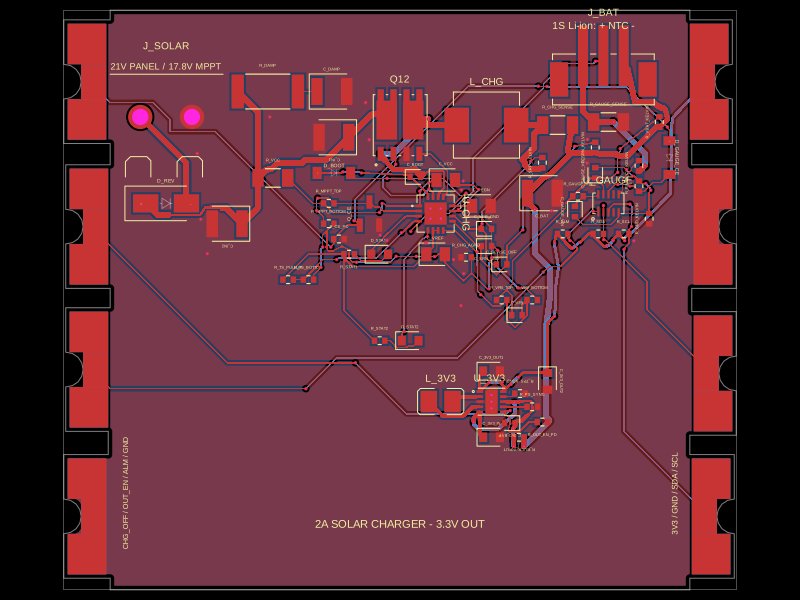 Similar packageShiboSoftwareDev/solar-battery-charger-moduleThis hardware setup integrates a solar panel, a lithium-ion battery, and a multi-rail buck converter with a battery charging IC, protection circuitry, and monitoring components, enabling solar power harvesting, battery charging, and power distribution in an embedded system.
 Discover something newimrishabh18/fitness_watchThis circuit integrates an ESP-12E microcontroller with various sensors and peripherals, including a AO3400A MOSFET for switching loads, to enable wireless control and sensor data processing.