pixalynx/pixal-gps
These files define two separate printed circuit boards: a small, two-layer battery cartridge with protection circuitry and contact pads for a pouch cell, and a larger, two-layer wireless charging dock featuring USB-C input, a resonant coil, and wireless power transmission components.
- Version
- 0.1.2
- License
- unset
- Stars
- 0
research/npm1300.md
# Nordic nPM1300 PMIC — fabrication-oriented research report

Compiled 2026-09-14 from official Nordic sources only (docs.nordicsemi.com, nordicsemi.com, devzone.nordicsemi.com
Nordic staff, Nordic's Azure download host, Nordic's GitHub). Every number carries a source tag; anything not found in a
fetched source is marked **UNVERIFIED**. Working copies of the downloaded files are in this directory
(`ek_hw/`, `qfn_ref/`, `nwp_050_hw_design_guidelines.pdf`, `npm1300_rev2_errata_v1.1.pdf`, `npm1300_ops_v0.7.pdf`,
`nrf_fuel_gauge.h`, extracted `.txt`/`.png` files).

## 0. Source index

| Tag | Document / page | URL |
|---|---|---|
| PS | nPM1300 Product Specification **v1.3 (March 2026)**, HTML | https://docs.nordicsemi.com/bundle/ps_npm1300/page/keyfeatures_html5.html |
| PS-REV | PS revision history (v1.0 Oct-2023 … v1.3 Mar-2026) | https://docs.nordicsemi.com/r/bundle/ps_npm1300/page/chapters/rev_history/1300_frontpage.html |
| PS-OV | PS Product overview (system electrical table: IQ, TSD, IOUTVSYS) | https://docs.nordicsemi.com/bundle/ps_npm1300/page/product_overview.html |
| PS-AMR | PS Absolute maximum ratings | https://docs.nordicsemi.com/r/bundle/ps_npm1300/page/chapters/abs_max_ratings/doc/abs_max_ratings.html |
| PS-ROC | PS Recommended operating conditions | https://docs.nordicsemi.com/r/bundle/ps_npm1300/page/chapters/recommended_op_conditions/doc/recommended_op_conditions.html |
| PS-SYSREG | PS SYSREG (VBUS input, current limiter, USB-C, VBUSOUT) | https://docs.nordicsemi.com/bundle/ps_npm1300/page/vbusin.html |
| PS-CHG | PS CHARGER | https://docs.nordicsemi.com/bundle/ps_npm1300/page/chapters/charger.html |
| PS-BUCK | PS BUCK | https://docs.nordicsemi.com/bundle/ps_npm1300/page/chapters/core_components/buck/doc/frontpage.html |
| PS-LDO | PS LOADSW/LDO | https://docs.nordicsemi.com/r/bundle/ps_npm1300/page/chapters/core_components/loadsw/doc/frontpage.html |
| PS-LED | PS LEDDRV | https://docs.nordicsemi.com/r/bundle/ps_npm1300/page/chapters/core_components/leddrv/doc/frontpage.html |
| PS-GPIO | PS GPIO | https://docs.nordicsemi.com/r/bundle/ps_npm1300/page/chapters/core_components/gpio/doc/frontpage.html |
| PS-ADC | PS System Monitor (ADC) | https://docs.nordicsemi.com/bundle/ps_npm1300/page/chapters/core_components/saadc/doc/frontpage.html |
| PS-POF | PS POF | https://docs.nordicsemi.com/r/bundle/ps_npm1300/page/chapters/core_components/plw/doc/frontpage.html |
| PS-SHIP | PS Ship and Hibernate modes | https://docs.nordicsemi.com/r/bundle/ps_npm1300/page/chapters/core_components/ship/doc/ship-mode.html |
| PS-RESET | PS RESET | https://docs.nordicsemi.com/r/bundle/ps_npm1300/page/chapters/core_components/reset/doc/frontpage.html |
| PS-TWI | PS TWI (+ electrical spec page …/twi_elspec.html) | https://docs.nordicsemi.com/r/bundle/ps_npm1300/page/chapters/core_components/ctrl_reg/doc/frontpage.html |
| PS-APP | PS Application | https://docs.nordicsemi.com/r/bundle/ps_npm1300/page/chapters/application/frontpage.html |
| PS-PIN | PS Pin assignments (QFN32 + CSP) | https://docs.nordicsemi.com/bundle/ps_npm1300/page/pin.html |
| PS-MECH | PS Mechanical specifications (read via browser, raw table) | https://docs.nordicsemi.com/bundle/ps_npm1300/page/chapters/hw_layout/mech_spec/frontpage.html |
| PS-REF | PS Reference circuitry | https://docs.nordicsemi.com/r/bundle/ps_npm1300/page/chapters/hw_layout/ref_circuitry/frontpage.html |
| PS-ORD | PS Ordering information | https://docs.nordicsemi.com/r/bundle/ps_npm1300/page/chapters/ordering_info/doc/ordering_info.html |
| PS-PDF | PS PDF attachment (Cloudflare-gated; **not retrievable** by curl/WebFetch) | https://docs.nordicsemi.com/viewer/book-attachment/ZO1FVHHS04YNNMSlbsZ0Kg/KbFbu1gXgIMOyTgBK7q46A-ZO1FVHHS04YNNMSlbsZ0Kg |
| OPS07 | nPM1300 **Objective** PS v0.7 (4490_280, 2023-06-26), Nordic-hosted on DevZone; used only for the charger electrical table the HTML PS omits | https://devzone.nordicsemi.com/cfs-file/__key/communityserver-discussions-components-files/4/nPM1300_5F00_OPS_5F00_v0.7.pdf |
| HDG | nPM1300 & nPM1304 Hardware Design Guidelines, nwp_050 (4490_475, 2025-08-20), HTML + PDF (local copy extracted) | https://docs.nordicsemi.com/bundle/nwp_050/page/WP/nwp_050/intro.html ; https://www.nordicsemi.com/-/media/Software-and-other-downloads/Product-Briefs/nwp_050.pdf |
| EKUG | nPM1300 EK Hardware user guide (HTML, rev April 2024; PDF v1.1.0) | https://docs.nordicsemi.com/bundle/ug_npm1300_ek/page/UG/nPM1300_EK/intro.html ; https://www.nordicsemi.com/-/media/Software-and-other-downloads/Product-Briefs/nPM1300_EK_User_Guide_v1.1.0.pdf |
| EKHW | nPM1300 EK hardware files 1.1.0 (PCA10152; schematic PDF `Schematic_Layout pdf files/PCA10152_Schematic_And_PCB.pdf`, BOM, Gerbers) | https://nsscprodmedia.blob.core.windows.net/prod/software-and-other-downloads/dev-kits/npm1300-ek/npm1300-evaluation-kit---hardware-files-1_1_0.zip |
| REFQFN | nPM1300-QEAA reference layout **v1.2 (2025-06-05)**: 4 configs, schematics/PCB PDFs, BOM xlsx, Gerbers, Altium | https://nsscprodmedia.blob.core.windows.net/prod/software-and-other-downloads/reference-layouts/npm1300/qfn/npm1300-qeaa-reference-layout-1_2.zip |
| ERR2 | nPM1300 Revision 2 Errata v1.1 (4490_604, 2025-10-21) | https://www.nordicsemi.com/-/media/Software-and-other-downloads/Product-Briefs/nPM1300_Rev_2_Errata_v1.1.pdf |
| ERR1 | nPM1300 Revision 1 Errata (HTML) | https://docs.nordicsemi.com/bundle/errata_nPM1300_Rev1/page/ERR/nPM1300/Rev1/latest/err_300.html |
| FAQ | DevZone blog "FAQ for the nPM1300 and nPM1304", Tomi Koskela (Nordic), 28 Jan 2026 | https://devzone.nordicsemi.com/nordic/nordic-blog/b/blog/posts/frequently-asked-questions-for-the-npm1300-and-npm1304 |
| DZ-DC | DevZone "Using nPM1300 with fixed DC input (no USB)" — answer by Tomi Koskela (Nordic) | https://devzone.nordicsemi.com/f/nordic-q-a/125077/using-npm1300-with-fixed-dc-input-no-usb |
| DZ-OTP | DevZone "nPM1300 VBUS input current limit OTP configuration" — Priyanka (Nordic) | https://devzone.nordicsemi.com/f/nordic-q-a/121255/npm1300-vbus-input-current-limit-otp-configuration |
| DZ-IQ | DevZone "nPM1300 Quiescent Current" — Håkon Alseth (Nordic) | https://devzone.nordicsemi.com/f/nordic-q-a/113825/npm1300-quiescent-current |
| DZ-VSYS | DevZone "nPM1300 max battery discharge current (Vsys)" — Ketiljo/Dacr (Nordic) | https://devzone.nordicsemi.com/f/nordic-q-a/113557/npm1300-max-battery-discharge-current-vsys |
| DZ-SHIP | DevZone "nPM1300 does not exit ship hold mode…" — Tomi Koskela | https://devzone.nordicsemi.com/f/nordic-q-a/123944/npm1300-does-not-exit-ship-hold-mode-when-shphld-button-pressed-or-vbus-connected/554437 |
| DZ-BTN | DevZone "Modifying the nPM1300 one button example" — Andy Sinclair (Nordic) | https://devzone.nordicsemi.com/f/nordic-q-a/110205/modifying-the-npm1300-one-button-example |
| DZ-REV | DevZone "nPM1300 + nRF54 module Hardware review" — Asbjørn (Nordic) | https://devzone.nordicsemi.com/f/nordic-q-a/129008/npm1300-nrf54-module-hardware-review/571160 |
| DZ-35U | DevZone "35uA ship mode current with nPM1300" — Asbjørn/Runar (Nordic) | https://devzone.nordicsemi.com/f/nordic-q-a/120983/35ua-ship-mode-current-with-nm1300 |
| NAN045 | App note "Using the nPM1300 and nPM1304 Fuel Gauge" (nan_045) | https://docs.nordicsemi.com/bundle/nan_045/page/APP/nan_045/intro.html (+ …/npm1300_fuel_gauge.html, …/power_consumption.html, …/fg_configuration_sleep.html) |
| FGLIB | nRF Fuel Gauge library README + `nrf_fuel_gauge.h` (nrfconnect/sdk-nrfxlib on GitHub) | https://nrfconnectdocs.nordicsemi.com/ncs/latest/nrfxlib/nrf_fuel_gauge/README.html ; https://raw.githubusercontent.com/nrfconnect/sdk-nrfxlib/main/nrf_fuel_gauge/include/nrf_fuel_gauge.h |
| NDOC | nordicsemi.com nPM1300 Documentation / Downloads pages (lists Design Checklist xlsx, errata, HDG PDF) | https://www.nordicsemi.com/Products/nPM1300/Documentation ; https://www.nordicsemi.com/Products/nPM1300/Downloads |
| JLC | JLCPCB parts API (queried 2026-09-14) | https://jlcpcb.com/api/overseas-pcb-order/v1/shoppingCart/smtGood/selectSmtComponentList |
| LCSC | LCSC product pages C7501206 / C7466043 / C25346894 | https://www.lcsc.com/product-detail/C7501206.html etc. |
| JLCS | jlcsearch.tscircuit.com | https://jlcsearch.tscircuit.com/components/list?search=nPM1300 |
| EE | EasyEDA/JLC footprint API | https://easyeda.com/api/products/C7501206/components?version=6.4.19.5 |

Not retrieved (Cloudflare-gated binary): the **nPM1300 Design Checklist (xlsx)** at
https://docs.nordicsemi.com/viewer/book-attachment/wH7wkdiGOzdx8uWOS_25TQ/r6fDKfk7npZLmz_21kbITA-wH7wkdiGOzdx8uWOS_25TQ [NDOC].

---

## 1. Package options, QFN variant, pin table

**Ordering codes** [PS-ORD]: package code **QE = QFN 5.0×5.0 mm, 32 pins, 0.5 mm pitch**; **CA = CSP (WLCSP) 3.1×2.4 mm,
35 balls, pitch 0.419–0.440 mm**. Containers: R7 = 7" reel, R = 13" reel. Order codes / MOQ: nPM1300-QEAA-R7 (1,500),
nPM1300-QEAA-R (4,000), nPM1300-CAAA-R7 (1,500), nPM1300-CAAA-R (7,000). Build code `<H><P><F>` (HW version /
production config / FW). MSL: QFN Level 2, CSP Level 1; ESD HBM 2 kV (class 2), CDM 500 V; storage −40…+125 °C [PS-AMR].
Silicon revisions: Revision 1 = build codes QEAA-C00 / CAAA-C00 [ERR1]; Revision 2 = QEAA-D00 / CAAA-D00 [ERR2].

**QFN32 mechanical (PS Table 1, mm, min/nom/max)** [PS-MECH]: A 0.8/0.85/0.9; A1 0/0.035/0.05; A2 –/0.65/–;
A3 –/0.08/–; A4 –/0.203/–; b (lead width) 0.2/0.25/0.3; D,E 4.9/5.0/5.1; **D2,E2 (exposed pad) 3.4/3.5/3.6**;
e (pitch) 0.5; K 0.35; L (lead length) 0.3/0.4/0.45. Marking/figure: PS Ordering info.

**CSP/WLCSP mechanical (PS Table 2, mm)** [PS-MECH]: A 0.416/0.464/0.512; A1 0.14/–/0.2; A2 0.254/0.269/0.284;
A3 –/0.05/–; A5 0.022/0.025/0.028; D 3.0475/3.0775/3.1075; D2 2.514; d 0.419; E 2.3475/2.3775/2.4075; E2 1.76;
e 0.44; F 0.88; G 1.257; ball b 0.195/–/0.255. (5×7 array: 4×0.44 = 1.76 = E2, 6×0.419 = 2.514 = D2 — i.e. pitch
0.44 mm across the 5-ball direction and 0.419 mm across the 7-ball direction; JLC/EasyEDA footprint name
"BGA-35_L3.1-W2.4-R5-C7-P0.42" agrees [EE].)

**QFN land pattern actually used by Nordic** (parsed from the reference-layout Gerbers, config 1, Altium footprint
`Nordic_QFN50P500X500X90-33N`) [REFQFN]:
- 32 oblong pin lands **0.30 × 0.851 mm**; land centres at ±0.249, ±0.749, ±1.25, ±1.75 mm along each side (0.5 mm pitch),
  outer-row centre at **±2.451 mm** from package centre (land spans 2.026 → 2.877 mm, i.e. ~0.38 mm beyond the 5.0 mm body).
- Exposed pad copper **3.5 × 3.5 mm** (= D2/E2 nominal); solder-mask opening 3.653 mm square; **paste: one full 3.5 mm
  square aperture** (100 % coverage in Nordic's stencil file).
- **9 thermal/ground vias (3×3, 1.2 mm pitch) inside the exposed pad: 0.305 mm (12 mil) drill, 0.61 mm pad**
  (drill report T2: 9 × 0.305 mm; the remaining 43 vias on the board are 0.249 mm drill / 0.50 mm pad).
- JLC/EasyEDA footprint for C7501206: "QFN-32_L5.0-W5.0-P0.50-TL-EP3.5", 33 pads, pin pads oval 0.80 × 0.28 mm, EP 3.5 mm [EE].

**QFN32 pin table** [PS-PIN]:

| Pin | Name | Type | Function |
|---|---|---|---|
| 1 | VOUT1 | Power | BUCK1 output |
| 2 | PVSS1 | Power | BUCK1 power ground |
| 3 | SW1 | Power | BUCK1 switch node to inductor |
| 4 | PVDD | Power | BUCK[n] power input (tie to VSYS) |
| 5 | SW2 | Power | BUCK2 switch node to inductor |
| 6 | PVSS2 | Power | BUCK2 power ground |
| 7 | GPIO0 | Digital I/O | GPIO0 |
| 8 | GPIO1 | Digital I/O | GPIO1 |
| 9 | GPIO2 | Digital I/O | GPIO2 |
| 10 | GPIO3 | Digital I/O | GPIO3 |
| 11 | GPIO4 | Digital I/O | GPIO4 |
| 12 | VDDIO | Power | Supply for TWI and GPIOs |
| 13 | SDA | Digital I/O | TWI data |
| 14 | SCL | Digital input | TWI clock |
| 15 | SHPHLD | Digital input | Ship mode hold (wake/reset button) |
| 16 | VSET2 | Analog input | Voltage set for BUCK2 (resistor to GND) |
| 17 | VSET1 | Analog input | Voltage set for BUCK1 (resistor to GND) |
| 18 | NTC | Analog input | Battery thermistor |
| 19 | VBAT | Power | Battery |
| 20 | VSYS | Power | System voltage output |
| 21 | VBUS | Power | Input supply |
| 22 | VBUSOUT | Analog output | VBUS output for host (USB detect) |
| 23 | CC1 | Analog input | USB Type-C configuration channel 1 |
| 24 | CC2 | Analog input | USB Type-C configuration channel 2 |
| 25 | LED0 | Analog output | LEDDRV0 output |
| 26 | LED1 | Analog output | LEDDRV1 output |
| 27 | LED2 | Analog output | LEDDRV2 output |
| 28 | LSIN1/VINLDO1 | Power | LOADSW1 supply or LDO1 input |
| 29 | LSOUT1/VOUTLDO1 | Power | LOADSW1 or LDO1 output |
| 30 | LSIN2/VINLDO2 | Power | LOADSW2 supply or LDO2 input |
| 31 | LSOUT2/VOUTLDO2 | Power | LOADSW2 or LDO2 output |
| 32 | VOUT2 | Power | BUCK2 output |
| EP (33) | AVSS | Power | Ground (exposed pad; "AVSS pin 33" in the reference schematics) |

WLCSP ball map (for reference) [PS-PIN]: A1 LED0, A2 LED1, A3 LED2, A4 LSOUT1/VOUTLDO1, A5 LSOUT2/VOUTLDO2, A6 AVSS,
A7 PVSS1; B1,B2 VBUS, B3 CC2, B4 LSIN1/VINLDO1, B5 LSIN2/VINLDO2, B6 VOUT1, B7 SW1; C1,C2 VSYS, C3 VBUSOUT, C4 GPIO3,
C5 GPIO2, C6 VOUT2, C7 PVDD; D1,D2 VBAT, D3 NTC, D4 SHPHLD, D5 CC1, D6 GPIO0, D7 SW2; E1 VSET2, E2 VSET1, E3 SCL,
E4 VDDIO, E5 SDA, E6 GPIO1, E7 PVSS2.

---

## 2. VBUS input, current limit, CC1/CC2

- Operating range **VBUSOP 4.0–5.5 V** [PS-ROC]; abs. max **VBUS −0.3…+22 V** (VBAT/VSYS/PVDD/VDDIO and all analog
  pins −0.3…+5.5 V; digital pins −0.3…VDDIO+0.3 V) [PS-AMR]. "22 V tolerant" [PS].
- SYSREG thresholds [PS-SYSREG electrical table]: **VBUSOVP 5.5 V** (SYSREG disabled above it, isolating VBUS);
  **VBUSMIN 3.6 V** (undervoltage with VBAT present); VBUSPOR 3.9 V (POR release); VBUSBOR 3.8 V (brown-out, no VBAT);
  **VBUSVALIDR 210 mV / VBUSVALIDF 160 mV** (VBUS must exceed VBAT by this to be used); RON VBUS→VSYS 300 mΩ (at 1.5 A);
  VBUSOUT switch 7.5 Ω (35 kΩ pull-down when off); ISUSP 1.8 mA (suspend); CC pull-downs Rd 5.1 kΩ; VRDCONN 0.2 V,
  VRD1A5 0.66 V, VRD3A 1.23 V; tRDDEB 15 ms.
- **Input current limit**: default at start-up **100 mA** (VBUSINILIMSTARTUP reset 0x01 = 100MA; factory OTP, not
  user-changeable [DZ-OTP]). Programmable via **VBUSINILIM0** (reset 0x01): 0 = 500MA0, 1 = 100 mA, 2 = 200 mA … 5 = 500 mA
  … **15 = 1500 mA** (100 mA steps). The new value takes effect only when **TASKUPDATEILIMSW = 1** is written
  ("SELVBUSILIM0"). The limit **reverts to 100 mA on reset and whenever the USB cable is unplugged and plugged back in**
  [PS-SYSREG]. Accuracy: only 100 mA and 500 mA are "USB-compliant, accurate" (IBUS100MA min 95 mA, IBUS500MA min
  495 mA); 600–1500 mA steps ±10 % [PS-SYSREG].
- **CC1/CC2**: USB-C charger detection comparators with internal 5.1 kΩ Rd; result is *only reported* in
  USBCDETECTSTATUS (NOCONNECTION / DEFAULTUSB / 1A5HIGHPOWER / 3AHIGHPOWER); **it never changes the limit
  automatically** — host reads it and sets VBUSINILIM0 [PS-SYSREG, FAQ, DZ-DC].
- **Non-USB-C 5 V source (e.g. wireless receiver)**: PS: "If USB Type-C configuration is not used, CC1 and CC2 can be
  left floating or connected to ground" [PS-SYSREG]; Nordic staff: "You can leave them floating" [DZ-DC].
  **To get 500 mA without CC**: after boot, host writes VBUSINILIM0 = 5 (500MA), then TASKUPDATEILIMSW = 1; repeat after
  every VBUS re-plug/reset [PS-SYSREG]. Before the host runs, the system sees only 100 mA — Nordic warns not to hang a
  >100 mA cold-start load on VSYS; gate loads with the load switches / keep bucks off until configured [DZ-OTP].
- Other VBUS facts: ~2.5 mA typ drawn from VBUS whenever VBUS is connected (references/oscillators), 1.8 mA in suspend
  (VBUSSUSPEND) [FAQ, PS-SYSREG]; no reverse-polarity protection — add external PMOS if needed [FAQ]; solar input not
  recommended [FAQ]. VBUSOUT (pin 22) is a protected copy of VBUS for the SoC's USB VBUS-detect; a **1 µF cap is required
  even if unused** [HDG §3.2.5]. The EK's PMIC USB-C port (J3) has **no TVS/ESD diode** on VBUS (the PRTR5V0U2X D1 on the
  EK sits on the nPM-Controller's separate USB port J4) [EKHW]; the reference layouts have no TVS either [REFQFN].
  HDG only says: 1 µF on VBUS, respect USB VBUS-capacitance limits, pick a cap rated for spikes (pin accepts 22 V) [HDG].

---

## 3. Charger, NTC/JEITA, thermal, ship mode / SHPHLD

**Charge current** [PS-CHG]: **32–800 mA in 2 mA steps**, set by registers **BCHGISETMSB/BCHGISETLSB** (9-bit; examples
32 mA = MSB 8/LSB 0, 400 mA = MSB 100, 800 mA = MSB 200), no sense resistor. Do not program outside the range.
**Termination voltage** BCHGVTERM (reset value 2 = **3.60 V default**): 3.50, 3.55, 3.60, 3.65 V then 4.00–4.45 V in
50 mV steps (values 4…13); BCHGVTERMR = separate VTERM for the *warm* region [PS-CHG]. VTERM accuracy ±1 % [OPS07].
**Trickle**: ITRICKLE = 10 % of ICHG while VBAT < VTRICKLE_FAST (**2.9 V default**, 2.5 V option, BCHGVTRICKLESEL);
**ITERM** = 10 % (default) or 20 % of ICHG (BCHGITERMSEL) [PS-CHG]. Charging will not start if VBAT < VBATLOW unless
BCHGVBATLOWCHARGE is set (VBATLOW value: **UNVERIFIED** — not in HTML PS; OPS07 lists VBATPOR 2.75 V / VBATBOR 2.4 V).
Recharge when VBAT < VRECHARGE (= **95 % of VTERM** per OPS07; DISABLERECHARGE in BCHGDISABLESET). Safety timers:
tOUTTRICKLE **10 min**, tOUTCHARGE **7 h** [OPS07 — values absent from HTML PS v1.3, treat as to-be-confirmed against PS PDF];
clear with TASKCLEARSAFETYTIMER. Charger drop-out VCHDROPOUT 50 mV, RON battery↔VSYS 160 mΩ [OPS07].
**Thermal regulation** [PS-CHG]: charging **stops** (not derates) when die temperature reaches TCHGSTOP and resumes at
TCHGRESUME; 10-bit DIETEMPSTOP/LSB (reset 0x5A/0x00 → code 360) and DIETEMPRESUME/LSB (reset 0x5D/0x00 → 372); PS Table 5:
435→50 °C, 397→80 °C, 372→100 °C, 359→110 °C; die-temp equation (PS image) **T_D[°C] = 394.67 − 0.7926·K_DIETEMP**
⇒ defaults ≈ **110 °C stop / 100 °C resume** (OPS07 states exactly 110 °C / 100 °C). Device thermal shutdown TSD 120 °C,
hysteresis 20 °C [PS-OV].
**Power path**: system load has priority; if load exceeds IBUSLIM the charge current is reduced; if still insufficient the
charger enters SUPPLEMENT mode taking battery current up to IBATLIM [PS-CHG].

**NTC / JEITA** [PS-CHG]: supported thermistors (PS Table 2): **10 kΩ ±1 %, β25/50 = 3380 K (β25/85 3434/3435 K)**;
47 kΩ, β 4050 K (4108 K); 100 kΩ, β 4250 K (4311 K). Select with ADCNTCRSEL (offset 0x0A in ADC bank): **0 = Hi_Z (no
thermistor), 1 = 10K, 2 = 47K, 3 = 100K** [PS-ADC] — set before enabling charging. NTC pin: thermistor from NTC to GND
(battery-pack NTC), the pull-up is internal (PS-ADC: "internal pull-up 10 kΩ/47 kΩ/100 kΩ, 1.5 V full scale" [FAQ]);
max **100 pF** in parallel with the thermistor. Default thresholds (PS Table 3, 10-bit codes; 10 kΩ / 47 kΩ / 100 kΩ):
**COLD 0 °C = 749/787/799 (NTCCOLD), COOL 10 °C = 658/684/693, WARM 45 °C = 337/306/297, HOT 60 °C = 237/197/186**.
Cold/hot: charging off; cool: 50 % ICHG (ICOOL) unless ENABLEFULLCHGCOOL; warm: VTERMR instead of VTERM (and optionally
disabled via BCHGCONFIG). Battery temperature from ADC: **T_BAT = 1 / (1/T0 − (1/β)·ln(1023/T_BATADC − 1))**, T0 = 298.15 K
[PS-ADC image]. During charging NTC is sampled automatically every 64/128/1024 ms and die temp every 4 ms
(TASKAUTOTIMUPDATE) [PS-ADC].
**No NTC**: "If a thermistor is not used, the NTC pin must be tied directly to ground or through a resistor. The
functionality must be disabled in register BCHGDISABLESET" [PS-CHG]; Nordic's minimal reference config 3 ties **NTC
directly to GND** [REFQFN]. The EK offers a 10 kΩ resistor (R9) to GND to emulate 25 °C; "if there is no NTC … and a
resistor is not connected between NTC and GND … charging will not occur" [EKUG ntc]. Rev-1 anomaly 36: packs whose PCM
needs > 0.95·VTERM to release will not charge — temporarily raise VTERM [ERR1].

**Ship mode / hibernate / SHPHLD** [PS-SHIP, PS-RESET]:
- Entry is **TWI-only** (TASKENTERSHIPMODE / TASKENTERHIBERNATE); the device enters immediately when VBUS is absent —
  software must wait for the VBUS-removed event before writing; no pin/voltage-based entry [PS-SHIP, FAQ].
- Ship/Hibernate "isolate the battery from the system" (VSYS → 0 V) [PS-SHIP, DZ-SHIP]; IQ **370 nA ship / 500 nA
  hibernate** [PS-OV]. Hibernate = ship mode + wake-up timer (TIMERHIBYTE/MID/LO + TIMERTARGETSTROBE).
- **SHPHLD pin**: internal **50 kΩ pull-up (RSHPHLD) to VBAT or VBUS, whichever is higher**; active low; VIL ≤ 0.4 V,
  VIH ≥ 1.2 V (to VBAT). Wake = hold low ≥ tshipToActive, configurable in SHPHLDCONFIG: 16/32/64/**96 (default)**/304/608/
  1008/3008 ms (apply with TASKSHPHLDCFGSTROBE). **VBUS > VBUSPOR (3.9 V) also wakes** the device. Long press
  ≥ **tRESETBUT = 10 s** → power cycle of the whole system (enabled by default, disableable; LPRESETCONFIG selects
  one-button SHPHLD or two-button SHPHLD+GPIO0).
- **Recommended button circuit**: momentary push-button from SHPHLD to GND, nothing else (EK: SW1 "PB SW" PTS810 directly
  between SHPHLD and GND; SW2 on GPIO0 for two-button reset; reference schematics bring SHPHLD out as a net only)
  [EKHW, REFQFN, EKUG buttons]. **Do not wire SHPHLD to a SoC GPIO** — the 50 kΩ pull-up leaks through the powered-down
  SoC's ESD diodes and drains the battery in ship mode; if the SoC needs the button, let the nPM1300 raise a GPIO
  interrupt on SHPHLD press/release instead [FAQ, DZ-35U]. Entering ship mode while the button is still held makes the
  device wake immediately (button becomes a wake source at entry) [DZ-BTN].

---

## 4. Power path / VSYS / VBAT

- VSYS is an **unregulated** rail: with VBUS valid (3.6 V < VBUS < 5.5 V and VBUS > VBAT + 210 mV rising / 160 mV falling)
  VSYS is VBUS through the 300 mΩ SYSREG switch ("supplies VSYS but does not regulate its voltage"); otherwise VSYS is VBAT
  through the charger path (RON 160 mΩ per OPS07) limited by IBATLIM [PS-SYSREG, PS-CHG].
- **IOUTVSYS: 1.0 A typ max DC load from battery (VBUS = 0), 1.5 A typ from VBUS/both** (VSYS > VSYSPOF) [PS-OV];
  Nordic staff: battery discharge limiter 1460 mA typ (IBATLIMHIGH) / 290 mA typ (IBATLIMLOW); driver constant 1340 mA
  max; exceeding it drops VSYS below VSYSPOF and resets the device — buffer inrush with VSYS capacitance [DZ-VSYS, FAQ].
  IBATLIM selection (PS Table 6): **IBATLIMLOW 200 mA (MSB 42/LSB 0)** for fuel-gauge accuracy when total load < 200 mA;
  **IBATLIMHIGH 1 A (MSB 207/LSB 1)** = default "High" [PS-CHG, DZ-VSYS].
- **VBATOP 2.3–4.45 V**; VDDIO 1.7 V–VSYS; TJ −40…+125 °C, TA −40…+85 °C [PS-ROC]. POF: VSYSPOF falling threshold default
  **2.7 V** (selectable 2.5/2.6…3.4/3.5 V, rising = +100 mV), warning on any GPIO, polarity selectable [PS-POF].
- "An application must not be supplied directly from VBAT … Use VOUT1, VOUT2, or VSYS" [PS-APP]. Supply-only options
  (no battery): PSU→VBAT with VBUS grounded (very low IQ, VBAT must stay < 4.65 V, no OVP) or PSU→VBUS with VBAT grounded
  (2.5 mA typ, full OVP, ≤ 5.5 V) [FAQ].

---

## 5. Regulators

**BUCK1/BUCK2** [PS-BUCK]: 1.0–3.3 V in 100 mV steps (BUCKnNORMVOUT; BUCK1NORMVOUT reset 0x02 = 1.2 V, BUCK2NORMVOUT reset
0x08 = 1.8 V, effective only after BUCKSWCTRLSEL selects software control); **200 mA max**; PVDD = VSYS, **min VSYS 2.7 V
to enable**; ±5 % accuracy; dropout 100 mV @ 1 mA; auto mode: hysteretic ↔ PWM at 90 mA / 40 mA; PWM **3.6 MHz**; ripple
5 mVpp (PWM, 200 mA) / 50 mVpp (hysteretic); efficiency 93 % (3.8 V→3.3 V @ 200 mA); start-up 1.2 ms (3.3 V, 10 µF);
active discharge 2 kΩ (BUCKCTRL0 pull-down enable); GPIO enable (BUCKENCTRL), forced PWM (BUCKPWMCTRL), retention voltage
(BUCKnRETVOUT via BUCKVRETCTRL GPIO). Above 200 mA the switch current limiter activates and VOUT sags with no host
notification [FAQ]. Hysteretic bucks cannot sink current — leakage from a higher rail makes VOUT rise [FAQ].
**VSET (resistor from pin to GND, ≤ 5 % tolerance, read only at power-on; pin must not float; < 100 Ω / grounded = buck
disabled)** [PS-BUCK, EKUG vset]:

| RVSET | VSET1 → VOUT1 | VSET2 → VOUT2 |
|---|---|---|
| < 100 Ω (GND) | 0 V (BUCK1 off) | 0 V (BUCK2 off) |
| 4.7 kΩ | 1.0 V | 1.8 V |
| 10 kΩ | 1.2 V | 2.0 V |
| 22 kΩ | 1.5 V | 2.2 V |
| **47 kΩ** | **1.8 V** | 2.4 V |
| 68 kΩ | 2.0 V | 2.5 V |
| 100 kΩ | 2.2 V | 2.7 V |
| 150 kΩ | 2.5 V | 3.0 V |
| **250–500 kΩ** | 2.7 V | **3.3 V** |

So **1.8 V = 47 kΩ on VSET1**; **3.3 V = 250–500 kΩ on VSET2** (BUCK1 cannot be pinned to 3.3 V by resistor — max 2.7 V;
Nordic's EK/reference use 47 kΩ → 1.8 V on BUCK1 and 150 kΩ → 3.0 V on BUCK2). "If resistor RVSETn is present, BUCK is
enabled with the output voltage defined by the resistor value" at power-on; afterwards **registers override**
(BUCKnNORMVOUT + BUCKSWCTRLSEL, or GPIO) [PS-BUCK]. Errata 27: do not switch to SW control while BUCKnNORMVOUT equals the
VSET-defined voltage (+1 mA IQ) [ERR2]; errata 28: force PWM/hysteretic if the auto-mode transition misbehaves [ERR2].
**Inductor**: **2.2 µH ±20 % only**; DCR ≤ 400 mΩ, Isat > 350 mA [PS-BUCK] / **Isat > 400 mA** [HDG §3.1]. HDG Table 1:
Taiyo Yuden LSCNB1608HKT2R2MD (1608, 0.8 mm, 292 mΩ), Taiyo Yuden MDKK1616T2R2MM (1616, 1.0 mm, 250 mΩ), TDK
VLS201610HBX-2R2M-1 (2016, 1.0 mm, 142 mΩ), TDK MLP2016H2R2MT0S1 (2016, 1.0 mm, 170 mΩ), **Samsung CIGT201610EH2R2MNE
(2016, 1.0 mm, 87 mΩ)**, Samsung CIGT252008LM2R2MNE (2520, 0.8 mm, 97 mΩ; best measured PWM efficiency 92.8 % @ 150 mA).
Nordic's EK and all reference-layout BOMs use **CIGT201610EH2R2MNE** (0806/2016, Isat 2.9 A, DCR 73 mΩ) [EKHW, REFQFN].
**Capacitors** [HDG §3.2, PS-BUCK]: buck output ≥ 4 µF effective (≤ 20 µF), ESR ≤ 50 mΩ, ≥ 6.3 V — nominal **10 µF 0603 X5R**
in reference; buck input **10 µF nominal per buck at PVDD** (≥ 4 µF eff.); VSYS **10 µF** extra; VBUS 1 µF; VBUSOUT 1 µF
(mandatory); VBAT **2.2 µF**; add 10–100 nF next to each 10 µF for RF-sensitive designs (config 4).

**LDO1/LDO2 / load switches** [PS-LDO, HDG §3.2.3]: pins LSIN1/VINLDO1 (28) → LSOUT1/VOUTLDO1 (29), LSIN2/VINLDO2 (30) →
LSOUT2/VOUTLDO2 (31); OFF at reset; **LDO mode**: VINLDO **2.6 V–VSYS**, 1.0–3.3 V in 100 mV steps, **50 mA (VOUT > 1.2 V) /
10 mA (VOUT < 1.2 V)**, dropout 25 mV typ, ±3 %, PSRR 50 dB, ripple 17/35 mVp-p (1.8/3.3 V), IQ +500 nA (hysteretic) /
+10 µA (PWM); output caps **2 × 10 µF nominal (≥ 6 µF effective)**. **Load-switch mode**: VINLS 1.0 V–VSYS, **100 mA**,
RDSON 200 mΩ (@3.3 V), soft-start 1.8 ms with limit 25/50/75/100 mA, pull-down 2 kΩ, IQ +60 nA; 1 µF output cap. GPIO
control by edge. Errata 38/40/41 (Rev 1 & 2): slow LDO start unless a TWI access follows; VINLDO droop at start (raise
VBUSINILIM0 ≥ 500 mA first, don't feed an LDO from a forced-PFM buck, stagger the two LDOs > 200 µs); LDO start can reset the
device if VBAT < VSYSPOF + 300 mV [ERR2]. Unused: reference config 3 ties **LSIN1/LSIN2 and LSOUT1/LSOUT2 to GND**, config 1
uses external VINLDO; PS text on unused pins: **UNVERIFIED**. Unused BUCK (config 3): VSET to GND, **VOUT1/VOUT2 tied to
VSYS/PVDD**, SW open, PVSS to GND [REFQFN].

---

## 6. Fuel gauge and measurements

- The fuel gauge is **host-side software**: the nRF Fuel Gauge library (nrfxlib, `nrf_fuel_gauge.h`) computes SOC (0–100 %),
  SOH, TTE/TTF from **battery voltage [V], current [A], temperature [°C]** and elapsed time, using a battery model
  generated by one-time profiling in nPM PowerUP (nRF Connect for Desktop) with the EK + nPM Fuel Gauge Board; init struct
  fields v0/i0/t0/model; "Current and voltage measurements do not have to be made at a certain interval … measured as
  closely as possible in time" [FGLIB]. "The host runs the fuel gauge algorithm and periodically requests measurements
  from the ADC" [PS-ADC]. Recommended cadence 1 s active / 5 s idle, ~500 ms while charging (SOH); cost 8–10 µA at 1 s
  (10.3 µC/iteration with NTC, 7.9 µC without) [NAN045]. Runs on nRF52/53/54/91 and third-party Cortex-M0/M0+/M3/M4/M33/M55
  or ESP32 Xtensa hosts [NAN045, FAQ]. Not coulomb counting — tolerant of pulsed loads; loads bypassing VSYS are unmetered [FAQ].
- **nPM1300 ADC** [PS-ADC]: 10-bit, tCONV 250 µs, DNL < 0.5 LSB; VBAT FS 5.0 V (±1 % for 3–4.5 V), VBUS FS 7.5 V (±1.5 %),
  VSYS FS 6.375 V (±1.5 %), NTC and die temp FS 1.5 V; **IBAT** FS = IBATLIM × 1.12 (discharge) or ICHG × 1.25 (charge)
  (ADCIBATMEASSTATUS), i.e. step ≈ IBATLIM/1024 — use IBATLIMLOW when load < 200 mA; not meaningful below ~5 mA [FAQ];
  VBAT burst mode (4 samples); single-shot/auto/timed modes.

---

## 7. Quiescent currents (PS system electrical table, all **typ**) [PS-OV]

IQSHIP **370 nA** (ship); IQSHIPT **500 nA** (hibernate); IQBAT battery operation, VBUS off: **600 nA** all BUCKs/LDOs off;
**800 nA** one BUCK auto, no load; **1.1 µA** both BUCKs auto, no load; **4.0 mA** one BUCK PWM 1.8 V; **7.1 mA** both PWM.
Adders: LDO 500 nA (hyst) / 10 µA (PWM); load switch 60 nA [PS-LDO]. With VBUS attached: 2.5 mA typ from VBUS, 1.8 mA in
suspend [FAQ, PS-SYSREG]. There is no separate "power-off" state: ship mode is the lowest (370 nA), lowest running sleep with
rails up ≈ 0.8–1.1 µA (auto mode, no load). Real boards often measure more: SHPHLD-to-SoC leakage, I²C pull-ups to a dead
VDDIO, floating GPIOs, Rev-1 anomaly 31 (+~300 µA below 20 mA hysteretic load, cleared by any TWI access) [DZ-IQ, DZ-35U, ERR1].

---

## 8. TWI, GPIO, LED pins

- TWI **7-bit address 0x6B (110 1011)**, fSCL 100 kHz min … 1000 kbps (table "Min 100 / Typ 1000 kbps"), tSU_DAT 50 ns,
  tHD_STA/tSU_STO 260 ns, tBUF 500 ns; **16-bit register address + 8-bit data** (bank in upper byte); supplied by **VDDIO
  (1.7 V–VSYS)** which must be present in all modes except ship/hibernate — recommended source VOUT1/VOUT2 [PS-TWI,
  PS-ROC, EKUG vddio]. Pull-ups external: reference schematics carry **optional 10 kΩ R1/R2 to VDDIO** [REFQFN]; VDDIO
  decoupling 100 nF (C13) [REFQFN]. (Internal SDA/SCL pull-ups: not documented — UNVERIFIED.)
- **GPIO0–4** [PS-GPIO]: reset = input with weak pull-down (GPIOMODE 0x00, GPIOPDEN 0x01, GPIOPUEN 0x00; ~500 kΩ);
  modes 0 GPIINPUT, 1 GPILOGIC1, 2 GPILOGIC0, 3 GPIEVENTRISE, 4 GPIEVENTFALL, **5 GPOIRQ (interrupt output)**, 6 GPORESET,
  7 GPOPLW (power-fail warning), 8 GPOLOGIC1, 9 GPOLOGIC0; drive 1/6 mA; open-drain option; 20 ms debounce; VIH 0.7·VDDIO,
  VIL 0.3·VDDIO. GPIOs can also enable BUCKs/LDOs, select retention voltage, force PWM, and GPIO0 is the second reset button.
  There is **no "ship-mode enable" GPIO** — entry is TWI only [FAQ].
- **LED0–2** [PS-LED, EKUG leds]: three low-side **5 mA constant-current** drivers, VLED 0.5 V–VSYS, anodes to **VSYS**,
  cathodes to LEDn, **no series resistor** in Nordic's reference (RGB LED directly VSYS→LEDn) [REFQFN]; modes 0 ERROR,
  1 CHARGING, 2 HOST (register-driven), 3 NOTUSED; reset: **LED0 = ERROR, LED1 = CHARGING, LED2 = HOST**; open-drain GP
  use needs an external pull-up.

---

## 9. Reference schematics — every external component

**Nordic reference layout nPM1300-QEAA v1.2, Config 1 "Full"** [REFQFN — schematic `npm1300_qeaa_config1_schematic.pdf`,
BOM `npm1300_qeaa_config1_bom.xlsx`]: C1 1.0 µF 10 V X5R 0603 (VBUS); C2, C3, C4 10 µF X5R ±20 % 0603 (VSYS/PVDD; C2→PVSS1,
C3→PVSS2, C4→GND); C5 1.0 µF (VBUSOUT); C6 **2.2 µF** X7R 16 V 0603 Taiyo Yuden EMK107BB7225KA-T (VBAT); L1, L2 2.2 µH
Samsung CIGT201610EH2R2MNE 0806 (SW1→VOUT1, SW2→VOUT2); C7, C8 10 µF (VOUT1 1.8 V, VOUT2 3.0 V, returned to PVSS1/PVSS2
with "Net tie" to GND and "Via to GND-layer on PVSSn"); C9–C12 10 µF (2 each on VOUTLDO1/2, VINLDO from external sources);
C13 100 nF 0201 (VDDIO); R1, R2 10 kΩ 0201 optional TWI pull-ups; **R3 47 kΩ (VSET1 → 1.8 V), R4 150 kΩ (VSET2 → 3.0 V)**;
LD1 RGB LED anodes to VSYS; J1 battery pack with NTC to NTC pin; CC1/CC2/SHPHLD/GPIO as nets. Config 2 "Simple": one buck
(C2, C4 10 µF; C5 1 µF VBUSOUT; C7 10 µF; L1), LOADSW1 fed from VOUT1 with C14 1.0 µF on LSOUT1, one green LED, R3 47 kΩ.
Config 3 "Minimal" (charger + VSYS only): C1 1 µF, C4 10 µF (VSYS), C5 1 µF (VBUSOUT), C6 2.2 µF, C13 100 nF, R1/R2 10 kΩ,
NTC→GND, VSET1/2→GND, VOUT1/VOUT2→VSYS, LSIN/LSOUT→GND. Config 4 = config 1 + 100 nF 0402 (Kemet C0402C104M4RAC7867)
on VSYS, PVDD-BUCK1 and BUCK2 supply for EMC. PS Reference circuitry chapter lists the same BOM: 10 µF X5R 25 V 0603,
1.0 µF X5R 10 V, 2.2 µF X7R 16 V, 100 nF 0201, 2.2 µH DCR < 400 mΩ 0806, R3/R4 47 kΩ/150 kΩ ±1 % 0201 [PS-REF].

**nPM1300 EK (PCA10152 v1.1.0) PMIC section** [EKHW — `PCA10152_Schematic_And_PCB.pdf` sheet 2/3/4, BOM
`PCA10152_BOM_Web.xls`]: C1 1.0 µF (VBUS); C2, C3, C4 10 µF (VSYS/PVDD; BOM: Murata GRM188R61E106MA73J, X5R 25 V 0603);
C5 1.0 µF (VBUSOUT); **C6 4.7 µF (VBAT)** (EK uses 4.7 µF vs 2.2 µF in the reference/HDG); C7 + C10 10 µF (VOUT1);
C8 10 µF (VOUT2); C9 100 nF (VDDIO); L1, L2 2.2 µH CIGT201610EH2R2MNE; C13–C16 10 µF LDO bypass (jumpered in LDO mode);
R3 47 kΩ RSET1 → 1.8 V, R4 150 kΩ RSET2 → 3.0 V (jumpers P13/P14, or GND = off); R9 10 kΩ (on-board NTC substitute on P3),
R10 DNM custom; J1 JST SM02B-SRSS-TB (battery, no NTC), J2 JST SM03B-SRSS-TB (battery + NTC); J3 USB-C DX07S016JA3R1500
(VBUS, CC1, CC2 to PMIC; **no TVS**); P2 external VBUS header; SW1–SW4 PTS810 tactile (SW1 SHPHLD, SW2 GPIO0, SW3 GPIO1,
SW4 GPIO2); LD1/LD2/LD3 0603 LEDs (red/green/amber, anodes VSYS, via JP9–JP11); R1 DNM current-measurement shunt on VBAT.
The separate nPM-Controller USB port carries D1 PRTR5V0U2X ESD, C11 1 µF, C12 100 nF, R14/R15 5.1 kΩ CC pull-downs.
Schematic PDF: inside the EKHW zip (no standalone URL); user guide PDF: EKUG link above.

---

## 10. Layout guidance

From HDG §4 [HDG] and the reference layout [REFQFN]:
- Follow the reference schematic/layout closely, "especially for the buck regulators"; ≥ 4 layers recommended (reference
  config 1 is 4-layer: GTL/G1/G2/GBL); solid ground on layer 2 with thin prepreg; 2-layer possible for QFN only with solid
  ground under DC/DC input/output/switch paths.
- Bucks: input caps as close as possible to PVDD and power ground, short/wide traces on both cap terminals; minimise the
  loop around **PVDD, PVSS1/2, SW1/2**; place the inductor so current rotates the same way in both switching cycles; input
  and output cap grounds close together on the same top copper, strongly stitched to the plane; keep the plane intact under
  the PMIC (only short escape routing); no star grounding; keep VBUS/VBAT/AVSS decoupling away from switch currents.
- Nordic's reference PCB: L1/L2 (0806) sit directly beside SW1/SW2 with the VOUT caps next to them, PVSS1/PVSS2 each go to
  the ground plane through a via at the pin ("Via to GND-layer on PVSSn", schematic net-tie); exposed pad = AVSS with the
  **3×3 grid of 0.305 mm-drill / 0.61 mm-pad vias**, mask opening 3.653 mm, full-pad paste aperture (see §1).
- Trace/via: size high-current traces for max load; more/bigger vias; ground vias next to signal vias; via stitching.
- Nordic review remarks: three 10 µF on VSYS/PVDD for high loads; add more ground-plane stitching vias; keep the VOUT caps
  and 100 nF close; never let a cap straddle the SW→L path [DZ-REV].

---

## 11. Availability (2026-09-14)

| Part | LCSC # | Package | JLC lib | Stock (JLC API / LCSC page) | Price |
|---|---|---|---|---|---|
| **nPM1300-QEAA-R7** | **C7501206** | QFN-32-EP 5×5 | Extended | **0 / out of stock** (LCSC: 1500/reel) | LCSC $1.7552 @1, $1.6618 @100; JLC $1.7431 @1 |
| nPM1300-QEAA-R | C7466043 | QFN-32 5×5 | Extended | 0 / out of stock (4000/reel) | LCSC $1.5339 @1 |
| NPM1300-CAAA-R7 | C25346894 | WLCSP-35 2.4×3.1 | Extended | **1435 (JLC) / 1,268 (LCSC)** | $2.674 @1, $1.7415 @100 (JLC) |
| NPM1300-CAAA-R | C22399753 | WLCSP-35 | Extended | 0 | $3.67 @1 |
| "nPM1300-QEAAC0" (JLCPCB Assembly placeholder) | C9900192425 | QFN-32 | – | 0, min 439 | – |

- **jlcsearch.tscircuit.com returns no results** for nPM1300 / NPM1300 (`/components/list.json?search=nPM1300` → `[]`) [JLCS].
- JLCPCB/EasyEDA **does** have symbol+footprint for C7501206 ("QFN-32_L5.0-W5.0-P0.50-TL-EP3.5") and C25346894 [EE, JLC part
  page]; importable with tscircuit's easyeda converter. Datasheet copies: https://www.lcsc.com/datasheet/C7501206.pdf.
- Build code caution: Rev 1 silicon = *C00, Rev 2 = *D00 [ERR1, ERR2]; the EK v1.1.0 BOM is "nPM1300-QEAAC0".
- Nordic-recommended inductors at JLC [JLC]: TDK **VLS201610HBX-2R2M-1 C307853** (0806, 142 mΩ, Isat 1.7 A) stock 300
  (jlcsearch shows 1843), $0.068 @1; Taiyo Yuden **LSCNB1608HKT2R2MD C6079477** (0603, 292 mΩ) stock 2267, $0.23 @1;
  Samsung CIGT201610EH2R2MNE only as JLC placeholder C9900052214 (stock 0); Samsung CIGT252008LM2R2MNE C16195795 stock 0.
  In-stock 2.2 µH 0806 alternatives meeting Isat > 400 mA / DCR ≤ 400 mΩ: Murata DFE201612E-2R2M=P2 C337893 (30,370 pcs,
  116 mΩ, 2.4 A), Sunlord WPN201610H2R2MT C97005 (21,851, 170 mΩ), TDK TFM201610GHM-2R2MTAA C136243 (4,226, 152 mΩ),
  Murata DFE201612P-2R2M=P2 C79317 (8,799, 144 mΩ) — none Nordic-validated.

## Errata summary (for the design)

Rev 2 (QEAA-D00/CAAA-D00, errata v1.1 2025-10-21) [ERR2]: 27 (BUCK +1 mA if SW-control set with equal VOUT), 28 (auto-mode
transition spread; force mode), 38 (slow LDO start; issue a TWI access), 40 (VINLDO droop at LDO start; raise VBUSINILIM0
≥ 500 mA first, stagger LDOs > 200 µs), 41 (LDO start resets if VBAT < VSYSPOF + 300 mV). Rev 1 (QEAA-C00) additionally:
30/34 (BUCK accuracy), **31 (+~300 µA hysteretic IQ below 20 mA load; any TWI access clears)**, 32 (hyst. efficiency),
36 (PCM release voltage vs 0.95·VTERM) [ERR1].

## Items still UNVERIFIED / not retrievable
- Charger electrical-table values VRECHARGE (95 % VTERM), tOUTTRICKLE 10 min, tOUTCHARGE 7 h, VCHDROPOUT 50 mV,
  VBATPOR 2.75 V / VBATBOR 2.4 V, RONCHARGER 160 mΩ, VTERMACC ±1 %: only in the 2023 Objective PS v0.7 [OPS07]; the current
  HTML PS v1.3 links to a "charger_el_spec" section that is not rendered, and the PS PDF is Cloudflare-gated.
- VBATLOW numeric threshold; PS text for unused LSIN/LSOUT pins; internal TWI pull-ups (none documented).
- nPM1300 Design Checklist xlsx contents (URL known, download gated).
Related Packages
 More from this authorpixalynx/esp32-gps-cellular-trackerThis code defines a hardware layout comprising a Wi-Fi-enabled ESP32 module, GPS module, cellular GSM module, battery management components (including charger, protection circuits, and voltage regulators), USB-C connector, SIM card holder, RF components, and supporting passive components for a comprehensive GPS+Cellular tracker device.
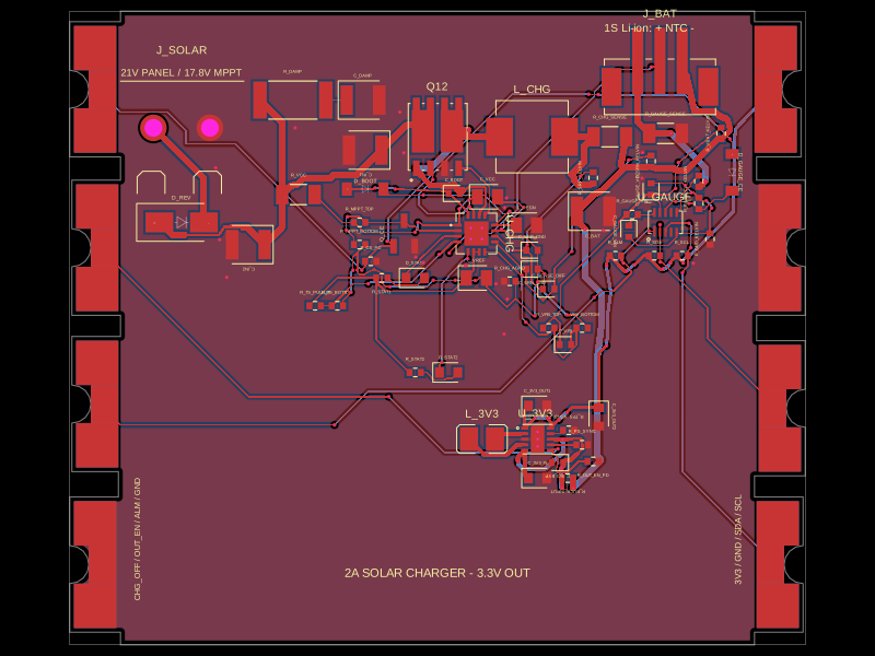 Similar packageShiboSoftwareDev/solar-battery-charger-moduleThis hardware setup integrates a solar panel, a lithium-ion battery, and a multi-rail buck converter with a battery charging IC, protection circuitry, and monitoring components, enabling solar power harvesting, battery charging, and power distribution in an embedded system.
 Discover something newimrishabh18/fitness_watchThis circuit integrates an ESP-12E microcontroller with various sensors and peripherals, including a AO3400A MOSFET for switching loads, to enable wireless control and sensor data processing.