pixalynx/pixal-gps
These files define two separate printed circuit boards: a small, two-layer battery cartridge with protection circuitry and contact pads for a pouch cell, and a larger, two-layer wireless charging dock featuring USB-C input, a resonant coil, and wireless power transmission components.
- Version
- 0.1.2
- License
- unset
- Stars
- 0
parts/RfFrontEnd.tsx
import type { ChipProps } from "tscircuit"
import { pad, via, outline, courtyard } from "../lib/footprints"

/** Skyworks SKY65943-11 GNSS LNA front-end module with integrated pre- and post-filters,
 * 10-pin MCM 2.5 x 2.5 mm (JLC C2654442). Pin table from the Skyworks datasheet 204404H
 * (docs/sources.md [sky65943]): 1 GND, 2 VEN, 3 VCC, 4 GND, 5 RF_IN, 6 GND, 7 FILT_OUT,
 * 8 AMP_IN, 9 GND, 10 RF_OUT, plus the ground paddle. Supply 1.62-3.3 V, 2.9 mA at 1.8 V,
 * 0.1 uA when VEN is low. The land pattern is the JLC/EasyEDA one: 0.30 x 0.50 mm lands on
 * a 0.5 mm pitch in two rows 2.4 mm apart, 0.52 mm-wide corner lands, 2.1 x 1.4 mm paddle. */
const Mcm10 = () => (
  <footprint>
    {pad(1, -1.144, -1.2, 0.52, 0.5)}
    {pad(2, -0.5, -1.2, 0.3, 0.5)}
    {pad(3, 0, -1.2, 0.3, 0.5)}
    {pad(4, 0.5, -1.2, 0.3, 0.5)}
    {pad(5, 1.144, -1.2, 0.52, 0.5)}
    {pad(6, 1.144, 1.2, 0.52, 0.5)}
    {pad(7, 0.5, 1.2, 0.3, 0.5)}
    {pad(8, 0, 1.2, 0.3, 0.5)}
    {pad(9, -0.5, 1.2, 0.3, 0.5)}
    {pad(10, -1.144, 1.2, 0.52, 0.5)}
    {pad(11, 0, 0, 2.1, 1.4)}
    {via(11, -0.55, 0, 0.25, 0.5)}
    {via(11, 0.55, 0, 0.25, 0.5)}
    {outline(2.5, 2.5)}
    <silkscreencircle pcbX={-1.75} pcbY={-1.6} radius={0.15} strokeWidth={0.1} />
    {courtyard(2.9, 2.9)}
  </footprint>
)
export const sky65943Pins = {
  pin1: ["GND1"], pin2: ["VEN"], pin3: ["VCC"], pin4: ["GND2"], pin5: ["RF_IN"], pin6: ["GND3"], pin7: ["FILT_OUT"],
  pin8: ["AMP_IN"], pin9: ["GND4"], pin10: ["RF_OUT"], pin11: ["GND_PAD"],
} as const
export const Sky65943 = (props: ChipProps<typeof sky65943Pins>) => (
  <chip
    {...props}
    manufacturerPartNumber="SKY65943-11"
    supplierPartNumbers={{ jlcpcb: ["C2654442"] }}
    pinLabels={sky65943Pins}
    internallyConnectedPins={[["GND1", "GND2", "GND3", "GND4", "GND_PAD"]]}
    footprint={<Mcm10 />}
    cadModel={{ objUrl: "https://modelcdn.tscircuit.com/easyeda_models/assets/C2654442.obj?uuid=77bfbb36aeda4085ae11f0a14d6642aa", rotationOffset: { x: 0, y: 0, z: 0 }, positionOffset: { x: 0, y: 0, z: 0 } }}
    schWidth={2.8}
    schHeight={3}
    schPinArrangement={{
      leftSide: { direction: "top-to-bottom", pins: ["RF_IN", "VEN", "VCC"] },
      rightSide: { direction: "top-to-bottom", pins: ["RF_OUT", "FILT_OUT", "AMP_IN"] },
      bottomSide: { direction: "left-to-right", pins: ["GND1", "GND_PAD"] },
    }}
    pinAttributes={{ VCC: { requiresPower: true }, GND1: { requiresGround: true }, GND_PAD: { requiresGround: true }, VEN: { mustBeConnected: true }, FILT_OUT: { mustBeConnected: true }, AMP_IN: { mustBeConnected: true } }}
  />
)

/** TI TPD3F303 SIM-card EMI filter + ESD array, USON-8 with ground paddle 1.6 x 2.1 mm (DPV;
 * JLC C2865991). Pin table from TI SLLSEM8 (docs/sources.md [tpd3f303]): 1 DATA1_OUT,
 * 2 CLK_OUT, 3 DATA2_OUT, 4 NC, 5 VCC (ESD clamp only, the supply is not routed through the
 * device), 6 DATA2_IN, 7 CLK_IN, 8 DATA1_IN; paddle = GND, "connect ... to the printed circuit
 * board ground plane through vias directly under the package". The pi filters are 45 ohm (CLK)
 * and 100 ohm (DATA) series with ~20 pF shunt capacitance; OUT pins face the SIM socket. */
const Uson8Ep = () => (
  <footprint>
    {[1, 2, 3, 4].map((p, i) => pad(p, -0.75 + i * 0.5, -0.722, 0.28, 0.553))}
    {[5, 6, 7, 8].map((p, i) => pad(p, 0.75 - i * 0.5, 0.722, 0.28, 0.553))}
    {pad(9, 0, 0, 1.7, 0.4)}{/* paddle vias intentionally omitted: a via-bearing land cannot be a routing endpoint; the ground pour and an adjacent router via connect it */}
    {outline(2.1, 1.6)}
    <silkscreencircle pcbX={-1.35} pcbY={-1.1} radius={0.15} strokeWidth={0.1} />
    {courtyard(2.4, 2.1)}
  </footprint>
)
export const tpd3f303Pins = {
  pin1: ["DATA1_OUT"], pin2: ["CLK_OUT"], pin3: ["DATA2_OUT"], pin4: ["NC"], pin5: ["VCC"], pin6: ["DATA2_IN"], pin7: ["CLK_IN"], pin8: ["DATA1_IN"], pin9: ["GND"],
} as const
export const Tpd3f303 = (props: ChipProps<typeof tpd3f303Pins>) => (
  <chip
    {...props}
    manufacturerPartNumber="TPD3F303DPVR"
    supplierPartNumbers={{ jlcpcb: ["C2865991"] }}
    pinLabels={tpd3f303Pins}
    footprint={<Uson8Ep />}
    cadModel={{ objUrl: "https://modelcdn.tscircuit.com/easyeda_models/assets/C2865991.obj?uuid=8931da5bc9704afdbe04de1fc09f054d", rotationOffset: { x: 0, y: 0, z: 0 }, positionOffset: { x: 0, y: 0, z: 0 } }}
    schWidth={2.8}
    schHeight={3}
    schPinArrangement={{
      leftSide: { direction: "top-to-bottom", pins: ["DATA1_IN", "CLK_IN", "DATA2_IN", "VCC"] },
      rightSide: { direction: "top-to-bottom", pins: ["DATA1_OUT", "CLK_OUT", "DATA2_OUT", "NC"] },
      bottomSide: { direction: "left-to-right", pins: ["GND"] },
    }}
    pinAttributes={{ GND: { requiresGround: true }, VCC: { requiresPower: true }, NC: { doNotConnect: true } }}
  />
)

/** Panasonic EVQP7A01P side-actuated tactile switch, 3.5 x 3.6 x 1.35 mm (JLC C79167).
 * Four lands; pins 1/1' are one contact, 2/2' the other (EasyEDA pin 3 = 1', pin 4 = 2'). */
const EvqP7 = () => (
  <footprint insertionDirection="from_right" cutoutApertureDirection="from_right">
    {pad(1, -1.8, 0.725, 1.4, 1.05)}
    {pad(2, -1.8, -0.725, 1.4, 1.05)}
    {pad(3, 1.8, 0.725, 1.4, 1.05)}
    {pad(4, 1.8, -0.725, 1.4, 1.05)}
    {outline(3.5, 3.6)}
    {courtyard(5.0, 3.8)}
  </footprint>
)
export const tactPins = { pin1: ["A"], pin2: ["B"], pin3: ["A2"], pin4: ["B2"] } as const
export const TactSwitch = (props: ChipProps<typeof tactPins>) => (
  <chip
    {...props}
    manufacturerPartNumber="EVQP7A01P"
    supplierPartNumbers={{ jlcpcb: ["C79167"] }}
    pinLabels={tactPins}
    internallyConnectedPins={[["A", "A2"], ["B", "B2"]]}
    footprint={<EvqP7 />}
    cadModel={{ objUrl: "https://modelcdn.tscircuit.com/easyeda_models/assets/C79167.obj?uuid=86f037ec24a240509f30a5629d3af720", rotationOffset: { x: 0, y: 0, z: 0 }, positionOffset: { x: 0, y: 0, z: 0 } }}
    schWidth={1.6}
    schHeight={1.2}
    schPinArrangement={{ leftSide: { direction: "top-to-bottom", pins: ["A"] }, rightSide: { direction: "top-to-bottom", pins: ["B"] } }}
  />
)
Related Packages
 More from this authorpixalynx/esp32-gps-cellular-trackerThis code defines a hardware layout comprising a Wi-Fi-enabled ESP32 module, GPS module, cellular GSM module, battery management components (including charger, protection circuits, and voltage regulators), USB-C connector, SIM card holder, RF components, and supporting passive components for a comprehensive GPS+Cellular tracker device.
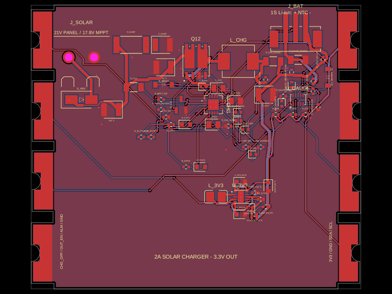 Similar packageShiboSoftwareDev/solar-battery-charger-moduleThis hardware setup integrates a solar panel, a lithium-ion battery, and a multi-rail buck converter with a battery charging IC, protection circuitry, and monitoring components, enabling solar power harvesting, battery charging, and power distribution in an embedded system.
 Discover something newimrishabh18/fitness_watchThis circuit integrates an ESP-12E microcontroller with various sensors and peripherals, including a AO3400A MOSFET for switching loads, to enable wireless control and sensor data processing.