pixalynx/pixal-gps
These files define two separate printed circuit boards: a small, two-layer battery cartridge with protection circuitry and contact pads for a pouch cell, and a larger, two-layer wireless charging dock featuring USB-C input, a resonant coil, and wireless power transmission components.
- Version
- 0.1.2
- License
- unset
- Stars
- 0
lib/passives.tsx
/** Compact helpers for two-terminal passives. Every part carries the JLCPCB part number
 * that the BOM will use; the mapping lives in one table so a value change is a one-line edit. */

export type Side = "top" | "bottom"
import type { ReactElement } from "react"
export type PassiveSpec = {
  name: string; value: string; x: number; y: number; rot?: number; side?: Side
  sch: [number, number]; section: string; footprint?: string | ReactElement; fpKey?: string; jlc?: string; dnp?: boolean; note?: string; schRot?: number
}

/** JLCPCB part numbers for the passive values used on the three boards (checked 2026-09-14
 * against jlcsearch.tscircuit.com; see docs/bom.md). Keys are `${value}@${footprint}`. */
export const JLC: Record<string, string> = {
  // capacitors
  "100nF@0402": "C1525", "1uF@0402": "C52923", "4.7uF@0402": "C82453", "10nF@0402": "C15195", "100pF@0402": "C1546",
  "22pF@0402": "C1555", "1nF@0402": "C1523", "2.2nF@0402": "C2987940", "22nF@0402": "C107026", "39pF@0402": "C1563",
  "10uF@0603": "C19702", "47uF@0805": "C2292827", "2.2uF@0603": "C23630", "10uF@0805": "C15850", "1uF@0603": "C15849",
  "470nF@0603": "C1623", "100nF@0603": "C14663", "10nF@0603": "C57112", "22nF@0603": "C106222", "56nF@0603": "C282072",
  "10uF@0402": "C15525", "2.2uF@0402": "C107369", "22uF@0805": "C45783", "15nF@0603": "C107076",
  // resistors
  "10k@0402": "C25744", "330@0402": "C25104", "68k@0402": "C2909379", "100k@0402": "C25741", "47k@0402": "C25792", "1k@0402": "C11702", "0@0402": "C17168",
  "1M@0402": "C26083", "20k@0402": "C25765", "68@0402": "C2909380", "200@0402": "C25087", "1.5k@0402": "C25867",
  "33k@0402": "C25779", "3.3k@0402": "C2909345", "100k@0603": "C25803", "1k@0603": "C21190", "10k@0603": "C2906982",
  "0.02@0805": "C601084", "5.1k@0402": "C25905", "2.2k@0402": "C25879",
  // inductors / beads
  "2.2uH@0806": "C337893", "1.5nH@0402": "C18221", "22nH@0402": "C12670", "9.1nH@0402": "C162547", "68nH@0402": "C108965",
  "FB22R@0603": "C710389", "FB120R@0402": "C85812",
}

const jlcFor = (p: PassiveSpec, fp: string | ReactElement) => p.jlc ?? JLC[`${p.value}@${typeof fp === "string" ? fp : p.fpKey ?? "custom"}`]

export const Cap = (p: PassiveSpec) => {
  const fp = p.footprint ?? "0402"
  const jlc = jlcFor(p, fp)
  return (
    <capacitor name={p.name} capacitance={p.value} footprint={fp} pcbX={p.x} pcbY={p.y} pcbRotation={p.rot ?? 0} layer={p.side ?? "top"}
      schX={p.sch[0]} schY={p.sch[1]} schRotation={p.schRot ?? 0} schSectionName={p.section} doNotPlace={p.dnp}
      supplierPartNumbers={jlc ? { jlcpcb: [jlc] } : undefined} />
  )
}
export const Res = (p: PassiveSpec) => {
  const fp = p.footprint ?? "0402"
  const jlc = jlcFor(p, fp)
  return (
    <resistor name={p.name} resistance={p.value} footprint={fp} pcbX={p.x} pcbY={p.y} pcbRotation={p.rot ?? 0} layer={p.side ?? "top"}
      schX={p.sch[0]} schY={p.sch[1]} schRotation={p.schRot ?? 0} schSectionName={p.section} doNotPlace={p.dnp}
      supplierPartNumbers={jlc ? { jlcpcb: [jlc] } : undefined} />
  )
}
export const Ind = (p: PassiveSpec) => {
  const fp = p.footprint ?? "0402"
  const jlc = jlcFor(p, fp)
  return (
    <inductor name={p.name} inductance={p.value} footprint={fp} pcbX={p.x} pcbY={p.y} pcbRotation={p.rot ?? 0} layer={p.side ?? "top"}
      schX={p.sch[0]} schY={p.sch[1]} schRotation={p.schRot ?? 0} schSectionName={p.section} doNotPlace={p.dnp}
      supplierPartNumbers={jlc ? { jlcpcb: [jlc] } : undefined} />
  )
}
/** Ferrite bead modelled as a chip so its value string ("22R@100MHz") is preserved in the BOM. */
export const Bead = (p: PassiveSpec & { mpn: string }) => {
  const fp = p.footprint ?? "0603"
  return (
    <chip name={p.name} manufacturerPartNumber={p.mpn} footprint={fp} pcbX={p.x} pcbY={p.y} pcbRotation={p.rot ?? 0} layer={p.side ?? "top"}
      schX={p.sch[0]} schY={p.sch[1]} schRotation={p.schRot ?? 0} schSectionName={p.section} pinLabels={{ pin1: ["A"], pin2: ["B"] }}
      schWidth={1} schHeight={0.6} schPinArrangement={{ leftSide: { direction: "top-to-bottom", pins: ["A"] }, rightSide: { direction: "top-to-bottom", pins: ["B"] } }}
      supplierPartNumbers={p.jlc ? { jlcpcb: [p.jlc] } : undefined} />
  )
}
Related Packages
 More from this authorpixalynx/esp32-gps-cellular-trackerThis code defines a hardware layout comprising a Wi-Fi-enabled ESP32 module, GPS module, cellular GSM module, battery management components (including charger, protection circuits, and voltage regulators), USB-C connector, SIM card holder, RF components, and supporting passive components for a comprehensive GPS+Cellular tracker device.
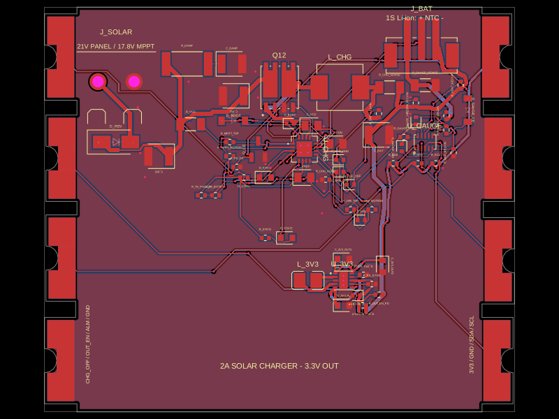 Similar packageShiboSoftwareDev/solar-battery-charger-moduleThis hardware setup integrates a solar panel, a lithium-ion battery, and a multi-rail buck converter with a battery charging IC, protection circuitry, and monitoring components, enabling solar power harvesting, battery charging, and power distribution in an embedded system.
 Discover something newimrishabh18/fitness_watchThis circuit integrates an ESP-12E microcontroller with various sensors and peripherals, including a AO3400A MOSFET for switching loads, to enable wireless control and sensor data processing.