pixalynx/pixal-gps
These files define two separate printed circuit boards: a small, two-layer battery cartridge with protection circuitry and contact pads for a pouch cell, and a larger, two-layer wireless charging dock featuring USB-C input, a resonant coil, and wireless power transmission components.
- Version
- 0.1.2
- License
- unset
- Stars
- 0
lib/footprints.tsx
import { Children, Fragment, type ReactElement } from "react"

/** Land-pattern generators. Every dimension is in millimetres and is annotated
 * with the manufacturer document it was read from (see docs/sources.md).
 * Pin numbering follows the manufacturer's pin table; pin 1 is top-left in the
 * unrotated footprint and numbering proceeds counter-clockwise for QFN/LGA
 * packages (left side downwards, bottom left-to-right, right upwards, top
 * right-to-left), which is the JEDEC convention used by Nordic, TI and ST. */

export const pad = (pin: number | string, x: number, y: number, w: number, h: number) => (
  <Fragment key={`p${pin}-${x}-${y}`}>
    <smtpad portHints={[typeof pin === "number" ? `pin${pin}` : pin]} pcbX={x} pcbY={y} width={w} height={h} shape="rect" />
  </Fragment>
)
export const circlePad = (pin: number | string, x: number, y: number, d: number) => (
  <Fragment key={`c${pin}-${x}-${y}`}>
    <smtpad portHints={[typeof pin === "number" ? `pin${pin}` : pin]} pcbX={x} pcbY={y} radius={d / 2} shape="circle" />
  </Fragment>
)
export const via = (pin: number | string, x: number, y: number, drill: number, padD: number) => (
  <Fragment key={`v${pin}-${x}-${y}`}>
    <platedhole portHints={[typeof pin === "number" ? `pin${pin}` : pin]} pcbX={x} pcbY={y} holeDiameter={drill} outerDiameter={padD} shape="circle" />
  </Fragment>
)
export const outline = (w: number, h: number, stroke = 0.12) => (
  <silkscreenpath route={[{ x: -w / 2, y: -h / 2 }, { x: w / 2, y: -h / 2 }, { x: w / 2, y: h / 2 }, { x: -w / 2, y: h / 2 }, { x: -w / 2, y: -h / 2 }]} strokeWidth={stroke} />
)
export const courtyard = (w: number, h: number) => (
  <courtyardoutline outline={[{ x: -w / 2, y: h / 2 }, { x: w / 2, y: h / 2 }, { x: w / 2, y: -h / 2 }, { x: -w / 2, y: -h / 2 }, { x: -w / 2, y: h / 2 }]} />
)
const pin1Mark = (x: number, y: number) => <silkscreencircle pcbX={x} pcbY={y} radius={0.15} strokeWidth={0.1} />

/** Generic QFN/DFN land pattern.
 * @param nx pins per horizontal side (top/bottom); @param ny pins per vertical side (left/right)
 * @param pitch pin pitch; @param span centre-to-centre distance of opposite land rows
 * @param landL land length (radial); @param landW land width (tangential)
 * @param ep exposed-pad copper size (0 = none); @param epVias grid of ground vias in the EP
 */
export function Qfn(p: { nx: number; ny: number; pitch: number; spanX: number; spanY?: number; landL: number; landW: number; ep?: number | [number, number]; epVias?: { n: number; pitch: number; drill: number; pad: number }; body: [number, number]; epPin?: number }) {
  const { nx, ny, pitch, spanX, landL, landW } = p
  const spanY = p.spanY ?? spanX
  const total = 2 * nx + 2 * ny
  const epPin = p.epPin ?? total + 1
  const pads: ReactElement[] = []
  let n = 1
  // left side, top to bottom
  for (let i = 0; i < ny; i++) pads.push(pad(n++, -spanX / 2, ((ny - 1) / 2 - i) * pitch, landL, landW))
  // bottom, left to right
  for (let i = 0; i < nx; i++) pads.push(pad(n++, (i - (nx - 1) / 2) * pitch, -spanY / 2, landW, landL))
  // right, bottom to top
  for (let i = 0; i < ny; i++) pads.push(pad(n++, spanX / 2, (i - (ny - 1) / 2) * pitch, landL, landW))
  // top, right to left
  for (let i = 0; i < nx; i++) pads.push(pad(n++, ((nx - 1) / 2 - i) * pitch, spanY / 2, landW, landL))
  const [epW, epH] = p.ep ? (Array.isArray(p.ep) ? p.ep : [p.ep, p.ep]) : [0, 0]
  const vias: ReactElement[] = []
  if (p.epVias && epW) {
    const { n: g, pitch: vp, drill, pad: vpad } = p.epVias
    for (let i = 0; i < g; i++) for (let j = 0; j < g; j++)
      vias.push(via(epPin, (i - (g - 1) / 2) * vp, (j - (g - 1) / 2) * vp, drill, vpad))
  }
  return (
    <footprint>
      {Children.toArray(pads)}
      {epW > 0 && pad(epPin, 0, 0, epW, epH)}
      {Children.toArray(vias)}
      {outline(p.body[0], p.body[1])}
      {pin1Mark(-p.body[0] / 2 - 0.45, p.body[1] / 2 - 0.1)}
      {courtyard(spanX + landL + 0.3, spanY + landL + 0.3)}
    </footprint>
  )
}

/** Nordic nPM1300 QFN32 5x5 mm, 0.5 mm pitch. Nordic reference layout v1.2 Gerbers
 * (Altium Nordic_QFN50P500X500X90-33N): 0.30 x 0.851 mm lands, row centres +/-2.451 mm,
 * exposed pad 3.5 mm (D2/E2 nominal 3.4-3.6), 9 ground vias 0.305 mm drill / 0.61 mm pad on
 * a 1.2 mm grid, mask opening 3.653 mm. Pin 1 top-left, numbering counter-clockwise (JLC
 * C7501206 footprint agrees on land order). */
export const Npm1300Qfn32 = () => (
  <Qfn nx={8} ny={8} pitch={0.5} spanX={4.902} landL={0.85} landW={0.30} ep={3.5} epVias={{ n: 3, pitch: 1.2, drill: 0.305, pad: 0.61 }} body={[5, 5]} />
)

/** TI BQ51013B VQFN-20 (RHL) 3.5 x 4.5 mm, 0.5 mm pitch: 8 lands on each long (4.5 mm) side,
 * 2 lands on each short side; thermal pad. Dimensions from TI RHL0020A land pattern
 * (see docs/sources.md, wireless-charging.md). Pin 1 = AC1 at the top-left corner of the
 * long side in the datasheet top view; here the long sides are horizontal. */
export const Bq51013bRhl = (p: { landL: number; landW: number; spanLong: number; spanShort: number; ep: [number, number] }) => {
  // TI numbers pins 1..8 along the bottom? No: RHL pin 1 is at the top-left of the package
  // when the 4.5 mm sides are vertical. We build it with the 4.5 mm sides vertical (ny=8, nx=2).
  return <Qfn nx={2} ny={8} pitch={0.5} spanX={p.spanShort} spanY={p.spanLong} landL={p.landL} landW={p.landW} ep={p.ep} epVias={{ n: 2, pitch: 1.0, drill: 0.25, pad: 0.5 }} body={[3.5, 4.5]} />
}

/** Nordic nRF9151 LGA-113, 12.1 x 11.1 x 1.2 mm. 80 perimeter lands on a 0.5 mm pitch
 * (20 per side; the four corner lands are 0.7 mm squares), 24 small reserved lands and
 * 9 large ground lands inside. Geometry as JLC/EasyEDA C22397843 (JLCPCB assembles from
 * this footprint) cross-checked against the Nordic product specification recommended
 * land pattern (docs/sources.md). Pin numbering follows Nordic: pin 1 is the top-left
 * corner land and numbering proceeds counter-clockwise around the perimeter (1-80), then
 * the inner lands 81-113. */
export function Nrf9151Lga113(p: { perimW?: number; perimL?: number; cornerSq?: number; innerSq?: number; gndSq?: number; edgeX?: number; edgeY?: number; cornerX?: number; cornerY?: number }) {
  const perimL = p.perimL ?? 0.45, perimW = p.perimW ?? 0.30, corner = p.cornerSq ?? 0.7, inner = p.innerSq ?? 0.2, gnd = p.gndSq ?? 1.6
  const edgeX = p.edgeX ?? 5.625, edgeY = p.edgeY ?? 5.125, cornerX = p.cornerX ?? 5.5, cornerY = p.cornerY ?? 5.0
  const pads: ReactElement[] = []
  let n = 1
  // Left column: pin 1 corner (top-left), pins 2-19 on x=-edgeX from y=+4.25 downwards, pin 20 corner (bottom-left)
  pads.push(pad(n++, -cornerX, cornerY, corner, corner))
  for (let i = 0; i < 18; i++) pads.push(pad(n++, -edgeX, 4.25 - i * 0.5, perimL, perimW))
  pads.push(pad(n++, -cornerX, -cornerY, corner, corner))
  // Bottom row: pins 21-40 on y=-edgeY from x=-4.75 to +4.75
  for (let i = 0; i < 20; i++) pads.push(pad(n++, -4.75 + i * 0.5, -edgeY, perimW, perimL))
  // Right column: pin 41 corner (bottom-right), 42-59 upwards, pin 60 corner (top-right)
  pads.push(pad(n++, cornerX, -cornerY, corner, corner))
  for (let i = 0; i < 18; i++) pads.push(pad(n++, edgeX, -4.25 + i * 0.5, perimL, perimW))
  pads.push(pad(n++, cornerX, cornerY, corner, corner))
  // Top row: pins 61-80 on y=+edgeY from x=+4.75 to -4.75
  for (let i = 0; i < 20; i++) pads.push(pad(n++, 4.75 - i * 0.5, edgeY, perimW, perimL))
  // Inner reserved lands 81-104 (0.2 mm squares): left column 81-89 (x=-4.10, y 3.40..-3.40 step 0.55/0.85 irregular
  // as EasyEDA/Nordic), centre rows 90-92 (y=-2.15) and 102-104 (y=+2.15), right column 93-101.
  const colY = [3.4, 2.85, 2.3, 0.55, 0, -0.55, -2.3, -2.85, -3.4]
  colY.forEach((y) => pads.push(pad(n++, -4.1, y, inner, inner)))            // 81-89
  ;[-0.55, 0, 0.55].forEach((x) => pads.push(pad(n++, x, -2.15, inner, inner))) // 90-92
  colY.slice().reverse().forEach((y) => pads.push(pad(n++, 4.1, y, inner, inner))) // 93-101 (bottom to top)
  ;[0.55, 0, -0.55].forEach((x) => pads.push(pad(n++, x, 2.15, inner, inner)))  // 102-104
  // Ground lands 105-113 (1.6 mm squares; 108 and 112 are 1.6 x 1.95)
  const gndLands: [number, number, number, number][] = [
    [-2.85, 2.85, gnd, gnd], [-2.85, 0, gnd, gnd], [-2.85, -2.85, gnd, gnd], [0, -3.575, gnd, 1.95],
    [2.85, -2.85, gnd, gnd], [2.85, 0, gnd, gnd], [2.85, 2.85, gnd, gnd], [0, 3.575, gnd, 1.95], [0, 0, gnd, gnd],
  ]
  gndLands.forEach(([x, y, w, h]) => pads.push(pad(n++, x, y, w, h)))
  // Ground vias in the large ground lands (one 0.3/0.6 via each; the SiP's GND lands
  // are the only path from the L1 pads to the L2 plane under the package).
  const gndVias = gndLands.map(([x, y], i) => via(105 + i, x, y, 0.3, 0.6))
  return (
    <footprint>
      {Children.toArray(pads)}
      {Children.toArray(gndVias)}
      {outline(12.1, 11.1)}
      {pin1Mark(-6.55, 5.55)}
      {courtyard(12.5, 11.5)}
    </footprint>
  )
}

/** Hirose U.FL-R-SMT-1 (Hirose drawing, matches JLC C88374): signal land 1.0 x 1.05 mm at
 * y=-1.05, two ground lands 1.05 x 2.2 mm at x=+/-1.475, y=+0.475. Cable exits along +y
 * from the receptacle; the signal pad is the "1" pin. Body 2.6 x 2.6 mm. */
export const UflRsmt = () => (
  <footprint insertionDirection="from_above">
    {pad(1, 0, -1.05, 1.0, 1.05)}
    {pad(2, -1.475, 0.475, 1.05, 2.2)}
    {pad(3, 1.475, 0.475, 1.05, 2.2)}
    {outline(2.6, 2.6)}
    {courtyard(4.2, 3.3)}
  </footprint>
)

/** ST LIS2DW12 LGA-12 2.0 x 2.0 x 0.7 mm, 0.5 mm pitch: 4 lands on the top/bottom edges
 * (x = +/-0.25, +/-0.75) and 2 on each side (y = +/-0.25). Land 0.28 x 0.50 mm, centres
 * 1.75 mm apart (JLC C189624; ST DS11473 Figure 12 gives the same 1.75 mm land rows). Pin 1
 * is the bottom-left land in ST's top view (marked corner), numbering counter-clockwise:
 * 1-4 bottom (left to right), 5-6 right (bottom to top), 7-10 top (right to left), 11-12 left
 * (top to bottom). */
export const Lga12_2x2 = () => (
  <footprint>
    {[-0.75, -0.25, 0.25, 0.75].map((x, i) => pad(1 + i, x, -0.875, 0.28, 0.5))}
    {pad(5, 0.875, -0.25, 0.5, 0.28)}
    {pad(6, 0.875, 0.25, 0.5, 0.28)}
    {[0.75, 0.25, -0.25, -0.75].map((x, i) => pad(7 + i, x, 0.875, 0.28, 0.5))}
    {pad(11, -0.875, 0.25, 0.5, 0.28)}
    {pad(12, -0.875, -0.25, 0.5, 0.28)}
    {outline(2, 2)}
    {pin1Mark(-1.35, -1.0)}
    {courtyard(2.5, 2.5)}
  </footprint>
)

/** 3215 (3.2 x 1.5 mm) two-pad 32.768 kHz crystal, e.g. Epson FC-135 / Seiko SC-32S.
 * Epson recommended land: 1.4 x 1.2 mm lands, 2.2 mm apart (centres +/-1.1). */
export const Crystal3215 = () => (
  <footprint>
    {pad(1, -1.1, 0, 1.4, 1.2)}
    {pad(2, 1.1, 0, 1.4, 1.2)}
    {outline(3.2, 1.5)}
    {courtyard(4.0, 2.0)}
  </footprint>
)

/** TI DRL (SOT-553) 5-lead, 1.6 x 1.2 mm body: lands 0.5 x 0.29 mm on a 0.5 mm pitch, rows
 * 1.4 mm apart (JLC C470828 / TI DRL0005A). Pin 1 top-left; pins 1-3 down the left, pin 4
 * bottom-right, pin 5 top-right. */
export const Sot553 = () => (
  <footprint>
    {pad(1, -0.7, 0.5, 0.5, 0.29)}
    {pad(2, -0.7, 0, 0.5, 0.29)}
    {pad(3, -0.7, -0.5, 0.5, 0.29)}
    {pad(4, 0.7, -0.5, 0.5, 0.29)}
    {pad(5, 0.7, 0.5, 0.5, 0.29)}
    {outline(1.6, 1.2)}
    {pin1Mark(-1.2, 0.8)}
    {courtyard(2.4, 1.9)}
  </footprint>
)

/** TI WSON-6 1.5 x 1.5 mm (DSE), 0.5 mm pitch: 0.75 x 0.28 mm lands, rows 1.27 mm apart
 * (JLC C183096). Pin 1 top-left, 1-3 down the left, 4-6 up the right. */
export const Wson6_1p5 = () => (
  <footprint>
    {pad(1, -0.636, 0.5, 0.75, 0.28)}
    {pad(2, -0.636, 0, 0.75, 0.28)}
    {pad(3, -0.636, -0.5, 0.75, 0.28)}
    {pad(4, 0.636, -0.5, 0.75, 0.28)}
    {pad(5, 0.636, 0, 0.75, 0.28)}
    {pad(6, 0.636, 0.5, 0.75, 0.28)}
    {outline(1.5, 1.5)}
    {pin1Mark(-1.15, 0.8)}
    {courtyard(2.3, 2.1)}
  </footprint>
)

/** Round ENIG contact pad for a spring-loaded (pogo) contact or test probe. */
export const ContactPad = (d = 2.0) => (
  <footprint>
    {circlePad(1, 0, 0, d)}
    <silkscreencircle pcbX={0} pcbY={0} radius={d / 2 + 0.25} strokeWidth={0.1} />
  </footprint>
)

/** Single-pad SMD spring-loaded pin such as BWCD-L3.5W2.0H1.0 (JLC C2826547): 2.0 mm base,
 * one 2.2 mm round land (EasyEDA), 3.5 mm free height, 1.0 mm stroke. */
export const PogoPinSmd = () => (
  <footprint insertionDirection="from_above">
    {circlePad(1, 0, 0, 2.2)}
    <silkscreencircle pcbX={0} pcbY={0} radius={1.4} strokeWidth={0.1} />
    {courtyard(2.6, 2.6)}
  </footprint>
)

/** 2.0 x 1.6 mm (0806 / 2016 metric) power inductor such as Murata DFE201612E / Samsung
 * CIGT201610: two 0.8 x 1.6 mm lands on 1.9 mm centres (Murata DFE201612E recommended pattern
 * 0.8 x 1.6, gap 1.1). */
export const Ind0806 = () => (
  <footprint>
    {pad(1, -0.95, 0, 0.8, 1.6)}
    {pad(2, 0.95, 0, 0.8, 1.6)}
    {outline(2.0, 1.6)}
    {courtyard(2.9, 2.0)}
  </footprint>
)
Related Packages
 More from this authorpixalynx/esp32-gps-cellular-trackerThis code defines a hardware layout comprising a Wi-Fi-enabled ESP32 module, GPS module, cellular GSM module, battery management components (including charger, protection circuits, and voltage regulators), USB-C connector, SIM card holder, RF components, and supporting passive components for a comprehensive GPS+Cellular tracker device.
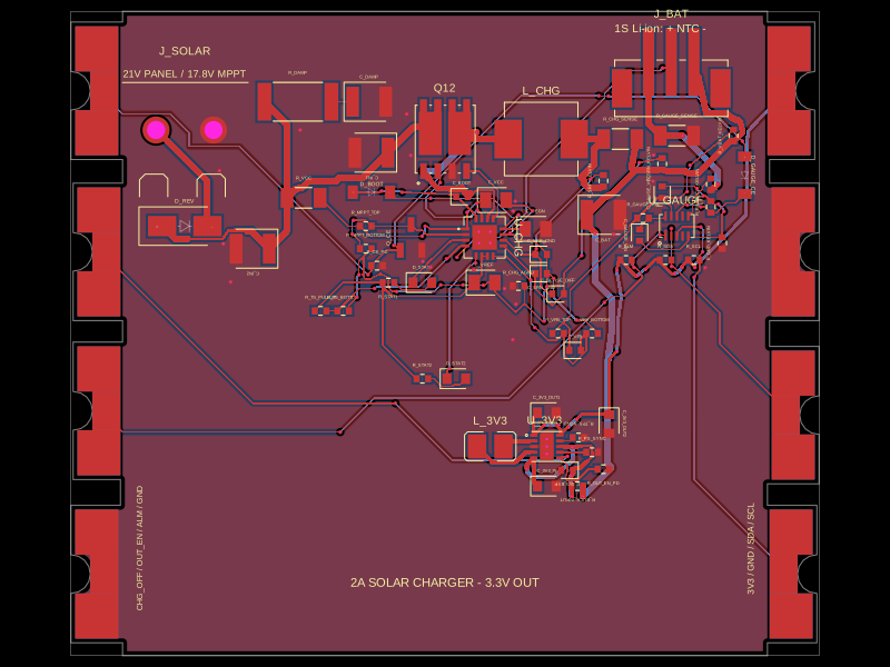 Similar packageShiboSoftwareDev/solar-battery-charger-moduleThis hardware setup integrates a solar panel, a lithium-ion battery, and a multi-rail buck converter with a battery charging IC, protection circuitry, and monitoring components, enabling solar power harvesting, battery charging, and power distribution in an embedded system.
 Discover something newimrishabh18/fitness_watchThis circuit integrates an ESP-12E microcontroller with various sensors and peripherals, including a AO3400A MOSFET for switching loads, to enable wireless control and sensor data processing.