pixalynx/pixal-gps
These files define two separate printed circuit boards: a small, two-layer battery cartridge with protection circuitry and contact pads for a pouch cell, and a larger, two-layer wireless charging dock featuring USB-C input, a resonant coil, and wireless power transmission components.
- Version
- 0.1.2
- License
- unset
- Stars
- 0
docs/stackup.md
# PCB stack-up, fabrication rules and impedance geometry

Reviewed 14 September 2026 against JLCPCB's published pages (URLs inline). Numbers marked "quote" were read from the live order form for a 4-layer 50 × 50 mm, 5-piece example and scale with area and quantity; re-quote before ordering.

## Decision: 4 layers, JLC04161H-7628, 1.6 mm (tracker A); 2 layers for the battery pack (B) and dock (C)

The tracker needs a 4-layer board. Reasons, in order of weight:

1. **RF reference.** Nordic's nRF9151 LTE (ANT) and GPS pins are 50 Ω ports. A continuous ground plane directly under the L1 RF traces and under the SiP is required for a defined 50 Ω line and for the SiP's ground return; a 2-layer 1.6 mm board would need a 2.8 mm-wide microstrip, which cannot exist between 0.5 mm-pitch pads.
2. **Density.** The nRF9151 has 80 perimeter lands on a 0.5 mm pitch plus 33 inner lands, the nPM1300 is a 0.5 mm QFN, the Qi receiver is a 0.5 mm QFN; escaping them on a ~32 × 24 mm board needs two routing layers besides the ground plane.
3. **Noise separation.** The nPM1300 buck converters, the Qi rectifier (110–205 kHz switching with harmonics) and the LTE PA share a board smaller than a postage stamp; the plane keeps their loops small.

| Layer | Use |
| --- | --- |
| L1 (top, 1 oz) | nRF9151, RF matching, U.FL connectors, crystal, decoupling; top ground pour (CPWG co-planar ground) |
| L2 (inner1, 0.5 oz) | Unbroken GND plane. RF reference. No signal routing. |
| L3 (inner2, 0.5 oz) | Power distribution (VSYS, VBAT, 1V8) and slow signals |
| L4 (bottom, 1 oz) | nano-SIM socket, nPM1300 + inductors, Qi receiver, accelerometer, battery pogo contacts, SWD/test pads; bottom ground pour |

Stack-up JLC04161H-7628 (https://jlcpcb.com/impedance): L1 0.035 mm Cu / prepreg 7628 0.2104 mm (Dk 4.4) / L2 0.0152 mm / core 1.065 mm (Dk 4.6) / L3 0.0152 mm / prepreg 7628 0.2104 mm / L4 0.035 mm; finished 1.59 mm ± 10 %. It is the only 4-layer stack-up JLCPCB tags "Standard" ("lowest cost and quickest turn-around", https://jlcpcb.com/pcb-impedance-calculator). Its L1–L2 spacing is identical on the 0.8 mm (JLC04081H-7628) and 1.0 mm (JLC04101H-7628) variants, so the board can be thinned later without changing the RF trace geometry.

Order-form settings: "Specify Stackup = Yes → JLC04161H-7628", "Impedance control = Yes (50 Ω single-ended, L1 ref L2)", surface finish **ENIG** (needed for the battery spring-contact pads, the pogo test pads and the LGA/QFN solder joints; quote +$16.80), via covering "Tented" (no via-in-pad is used: the nRF9151 land pattern leaves room for dog-bone vias, and 4-layer epoxy-filled vias cost about +$20 per order), min via 0.2 mm drill / 0.4 mm pad (inside JLCPCB's 0.15/0.25 minimum with the recommended ≥0.2 mm ring), track/space design floor 0.10/0.10 mm (JLCPCB minimum 0.09/0.09; https://jlcpcb.com/capabilities/pcb-capabilities). Hard gold is **not** offered by JLCPCB on the standard form (their gold fingers are ENIG); ENIG 2 µin is selectable after choosing ENIG and is the finish to order for the contact pads.

## 50 Ω geometry used on L1

JLCPCB's own calculator (https://jlcpcb.com/pcb-impedance-calculator, run 2026-09-14, includes their solder-mask and trapezoid model):

| Structure | Width | Gap to co-planar ground |
| --- | --- | --- |
| Microstrip, L1 over L2, 7628 | 0.359 mm | — |
| **CPWG, L1 over L2, 7628 (used)** | **0.32 mm** | **0.25 mm** |

Closed-form cross-checks (Hammerstad–Jensen microstrip 0.387 mm; Wadell conductor-backed CPW 0.389 mm at a 0.25 mm gap, no mask) agree within the ±10 % impedance tolerance JLCPCB controls to. The design draws the two RF lines (ANT → matching → U.FL LTE, GPS → SAW/LNA → matching → U.FL GNSS) at 0.32 mm with a 0.25 mm mask-defined gap to the top ground pour, ground-stitching vias along both sides on ≤ 1.5 mm pitch (λ/20 at 2.2 GHz in FR-4 is ≈ 4.8 mm), and no other copper on L1/L2 under or beside them.

## Assembly service

Two-sided assembly forces **Standard PCBA** (Economic is single-sided): setup $51.12 + stencil $16.42 for double-sided, $1.53 feeder fee per part, $0.0016 per joint, X-ray added automatically for the LGA/QFN parts (https://jlcpcb.com/help/article/pcb-assembly-price, https://jlcpcb.com/capabilities/pcb-assembly-capabilities). Standard PCBA accepts 0201 passives and 0.35 mm pitch; this design stays at 0402 and ≥ 0.5 mm pitch so a hand-rework is still possible. Minimum single-board size for Standard PCBA is 70 × 70 mm, so the 32 × 24 mm tracker must be ordered as a panel (JLCPCB panelises on request: "Panel by JLCPCB" with V-cut or stamp holes; tracker panels of 2 × 3 fit comfortably).

The nRF9151 is in JLCPCB's catalogue as an Extended part (C22397843, "LGA-113 (12.1×11.1)", "X-ray Inspection Required", MSL 3, https://jlcpcb.com/partdetail/24009643-nRF9151_LACAR7/C22397843).

## LTE and GNSS bands the antennas must cover

nRF9151 Cat-M1 bands 1, 2, 3, 4, 5, 8, 12, 13, 18, 19, 20, 25, 26, 28, 66, 85, 106 through "a single 50 Ω antenna pin", 700–2200 MHz (https://docs.nordicsemi.com/r/bundle/ps_nrf9151/page/nrf9151_html5_keyfeatures.html). The union is 699–960 MHz plus 1710–2200 MHz (3GPP TS 36.101 Table 5.5-1). GNSS is GPS/QZSS L1 C/A at 1575.42 MHz only; Nordic states "External low-noise amplifier (LNA) with SAW filter recommended on the GPS antenna input", "GPS antenna pin is DC grounded" and "minimum 27 dB attenuation to out of band power" (https://docs.nordicsemi.com/r/bundle/ps_nrf9151/page/gps.html).
Related Packages
 More from this authorpixalynx/esp32-gps-cellular-trackerThis code defines a hardware layout comprising a Wi-Fi-enabled ESP32 module, GPS module, cellular GSM module, battery management components (including charger, protection circuits, and voltage regulators), USB-C connector, SIM card holder, RF components, and supporting passive components for a comprehensive GPS+Cellular tracker device.
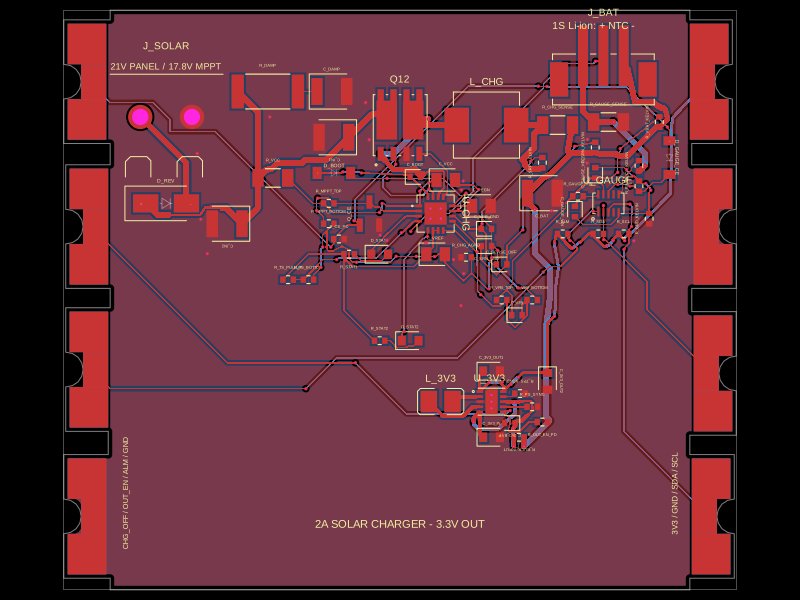 Similar packageShiboSoftwareDev/solar-battery-charger-moduleThis hardware setup integrates a solar panel, a lithium-ion battery, and a multi-rail buck converter with a battery charging IC, protection circuitry, and monitoring components, enabling solar power harvesting, battery charging, and power distribution in an embedded system.
 Discover something newimrishabh18/fitness_watchThis circuit integrates an ESP-12E microcontroller with various sensors and peripherals, including a AO3400A MOSFET for switching loads, to enable wireless control and sensor data processing.