pixalynx/pixal-gps
These files define two separate printed circuit boards: a small, two-layer battery cartridge with protection circuitry and contact pads for a pouch cell, and a larger, two-layer wireless charging dock featuring USB-C input, a resonant coil, and wireless power transmission components.
- Version
- 0.1.2
- License
- unset
- Stars
- 0
docs/battery-pack.md
# Removable battery cartridge (PCB B) and its mechanics

## Electrical contract between cartridge and tracker

Four gold pads on the cartridge, four spring contacts (BWCD-L3.5W2.0H1.0 pogo pins, JLC C2826547: Ø2.0 mm base, 3.5 mm free height, ~1 mm travel, 1.5 A, gold over brass) on the tracker, 3.0 mm pitch, order **BAT+ · GND · NTC · ID**.

| Contact | Cartridge side | Tracker side | Notes |
| --- | --- | --- | --- |
| BAT+ | cell positive (after the pack's own protection if the cell carries a PCM, otherwise directly) | nPM1300 VBAT (2.2 µF) | 0.5 A LTE pulses; contact resistance ≤ 30 mΩ per the pogo datasheet |
| GND | pack negative after the protection FETs | tracker ground | — |
| NTC | 10 kΩ β3380 NCP15XH103F03RC to pack GND | nPM1300 NTC pin (100 pF to GND) | nPM1300 `ADCNTCRSEL = 10K`; JEITA thresholds 0/10/45/60 °C by default |
| ID | resistor to pack GND | 100 kΩ series → nRF9151 AIN0; 100 kΩ pull-up driven from P0.14 only during a measurement | Nokia-style BSI: 68 kΩ → 600/650 mAh class (this pack); 47 k, 82 k, 100 k reserved for other capacities; open = no cartridge |

**Reverse insertion.** A cartridge rotated 180° in the slot presents the pads in the order ID · NTC · GND · BAT+. The tracker then sees: BAT+ contact → the pack's ID resistor (open circuit, harmless), GND contact → the NTC (harmless), NTC pin → pack GND (reads as a shorted thermistor, charger refuses to charge, no damage: the nPM1300 analogue pins are rated to 5.5 V), ID pin → pack BAT+ (up to 4.2 V through the 100 kΩ series resistor into a 1.8 V-rail input: ≤ 25 µA through the nRF9151 protection diode, allowed). No path applies reverse polarity to the PMIC and nothing is powered, so a reversed cartridge simply does nothing. Mechanical keying in the cartridge still prevents this in production; the electrical order is the second line of defence.

## Protection: one layer, not two

Every candidate cell (Honcell HCP503040NFC, Jauch LP503040JH, Renata ICP622540PMT, LiPol LP513040/LP603450) is normally sold with a certified protection module (PCM: S-8261 or DW01 class IC + 8205 dual FET, 2.8–3.0 V under-voltage, 4.25–4.30 V over-voltage, 1.5–3 A over-current, short-circuit). Putting a second protector in series would add ~50 mΩ, a second under-voltage cut-off that fights the first, and no safety benefit, so PCB B has **one** protection position and a jumper:

- `PROTECTION_ON_PACK = true` (default, production intent): buy the cell as a bare tabbed cell and populate U1 (TI BQ29700DSER: OVP 4.275 V/1.25 s, UVP 2.80 V/144 ms, OCD 100 mV/20 ms, SCD 0.5 V/250 µs, 4 µA) + Q1 (FS8205A common-drain dual N-MOSFET, 20 V, 6 A, 25 mΩ max at 4.5 V) with TI's reference values R1 330 Ω, C1 100 nF, R2 2.2 kΩ. OCD trips at 100 mV / (2 × 25 mΩ) ≈ 2 A, well above the 0.5 A LTE bursts. JP1 is not fitted.
- `PROTECTION_ON_PACK = false` (prototype with a PCM'd cell such as the Jauch part from Digi-Key): U1/Q1/R1/R2/C1 become DNP and JP1 (0 Ω, 0603) bridges CELL− to GND. The cell's own PCM is then the single protection layer.

The board is manufacturable on its own: 26 × 7 mm, 2 layers, 0.8 mm, ENIG (the contact pads are the outer-face ENIG lands, 2.4 mm diameter, ≥ 0.15 mm over the pogo tip diameter in every direction after ±0.5 mm cartridge play). JLCPCB does not offer hard gold; ENIG 2 µin is the finish to order (see [stackup.md](stackup.md)). With < 100 mating cycles expected over the life of a consumer tracker this is adequate; for a swap-daily product specify 30 µin hard gold at a board house that offers it.

## Cartridge dimensions (basis: Honcell HCP503040NFC / Jauch LP503040JH, 5.4 × 30.5 × 40.5 mm)

| Feature | Value | Reason |
| --- | --- | --- |
| Cell nominal | 5.4 × 30.5 × 40.5 mm (with PCM ≈ 42 mm long) | datasheets |
| Swelling allowance | +0.6 mm thickness (≈ 10 %), +0.3 mm width, +0.5 mm length | LiPo pouch cells grow with age; never clamp to zero clearance |
| PCB B | 26 × 7 × 0.8 mm across the tab end, components ≤ 1.0 mm tall on the cell side | sits in the 5.4 mm thickness beside the folded tabs |
| Inner cavity | 6.4 × 31.5 × 47 mm (cell + swelling + 5.5 mm for PCB B and tab fold + 0.5 mm foam) | — |
| Wall thickness | 0.8 mm (PC/ABS, injection) / 1.2 mm (SLA or FDM prototype) | shell ≥ 0.8 mm keeps the pouch from being punctured; no sharp PCB edge may touch the pouch: PCB B edges are chamfered and a 0.5 mm PU foam pad separates it from the cell |
| Outer envelope | ≈ 8.0 × 33.1 × 48.6 mm injection / 8.8 × 33.9 × 49.4 mm printed | — |
| Contact window | 4 pads on the outer face at the PCB end, 3.0 mm pitch, centred; window 14 × 3.5 mm | mates with the tracker's pogo row (bottom side of PCB A, along the top edge at y = +10.5 mm, x = −3, 0, +3, +6 mm) |
| Keying | one corner chamfer 2 × 45° plus a 1 mm rib along one long side | prevents 180° rotation and upside-down insertion |
| Retention | two snap hooks on the long sides engaging a 0.6 mm groove in the tracker shell; release by a thumb notch | spring-contact preload 0.5–1.0 mm (pogo travel 1 mm, working height 2.5 mm) |
| Insulation | pouch wrapped in 0.05 mm PET; tabs insulated with Kapton; PCB B conformal coated on the cell side | — |
| Venting | 2 × 0.5 mm slits at the far end | pressure relief if the pouch swells |

The cartridge cavity should be sized to the +swelling numbers, and the cell should be retained by foam pressure, not by rigid stops. The Qi receiver coil is **not** in the cartridge: it sits on the tracker's rear shell (behind the cartridge) so every cartridge stays a passive, cheap part.

## Firmware view

- Read ID: drive P0.14 high, wait 10 µs, sample AIN0 (10-bit, 40 µs acquisition), drive P0.14 low. V = 1.8 V × R_ID / (R_ID + 100 k): 68 k → 0.73 V; > 1.6 V → no cartridge (open); < 0.1 V → shorted ID.
- NTC is read by the nPM1300 (`ADCNTCRSEL = 10K`); the nRF Fuel Gauge library takes VBAT, IBAT and T from the PMIC.
- Firmware must set `IBATLIM` High (1 A) before enabling the modem, and should program `VTERM = 4.20 V`, `ICHG = 300 mA` for the 600 mAh cell.
Related Packages
 More from this authorpixalynx/esp32-gps-cellular-trackerThis code defines a hardware layout comprising a Wi-Fi-enabled ESP32 module, GPS module, cellular GSM module, battery management components (including charger, protection circuits, and voltage regulators), USB-C connector, SIM card holder, RF components, and supporting passive components for a comprehensive GPS+Cellular tracker device.
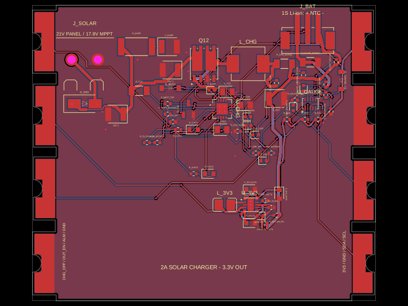 Similar packageShiboSoftwareDev/solar-battery-charger-moduleThis hardware setup integrates a solar panel, a lithium-ion battery, and a multi-rail buck converter with a battery charging IC, protection circuitry, and monitoring components, enabling solar power harvesting, battery charging, and power distribution in an embedded system.
 Discover something newimrishabh18/fitness_watchThis circuit integrates an ESP-12E microcontroller with various sensors and peripherals, including a AO3400A MOSFET for switching loads, to enable wireless control and sensor data processing.