pixalynx/pixal-gps
These files define two separate printed circuit boards: a small, two-layer battery cartridge with protection circuitry and contact pads for a pouch cell, and a larger, two-layer wireless charging dock featuring USB-C input, a resonant coil, and wireless power transmission components.
- Version
- 0.1.2
- License
- unset
- Stars
- 0
battery-pack.circuit.tsx
import { Fragment } from "react"
import { Bq29700, Fs8205a } from "./parts/Protection"
import { Contact } from "./parts/Connectors"
import { Cap, Res, type PassiveSpec } from "./lib/passives"
import { pad, outline, courtyard } from "./lib/footprints"
import { localPath, type Pt } from "./lib/geometry"

/**
 * PIXAL GPS battery cartridge PCB, board B (Rev A). 30 x 7 mm, 2 layers, 0.8 mm, ENIG.
 *
 * Sits across one end of the 503040-class pouch cell (30.5 mm wide) inside the plastic
 * cartridge. The four ENIG contact pads on the outer face mate with the tracker's spring
 * contacts in the order BAT+, GND, NTC, ID (3.0 mm pitch). The cell tabs solder to CELL+ /
 * CELL- at the left end. The protection (TI BQ29700 + FS8205A common-drain pair, TI
 * reference values) is populated for a bare tabbed cell; for a cell that already carries a
 * certified PCM set PROTECTION_ON_PACK = false: the protector parts become DNP and JP1
 * bridges CELL- to GND so the cell's own PCM is the single protection layer.
 *
 * All copper is explicit (pcbPath legs): the board is small enough that hand routing is
 * deterministic and DRC-clean, so the autorouter is disabled here. The bottom layer is a
 * ground pour reached through the stub vias.
 */
export const PROTECTION_ON_PACK = true
export const PACK_ID_OHMS = "68k" // Nokia-style BSI value: 68 k = 600/650 mAh class (docs/battery-pack.md)

const CONTACT_PITCH = 3.0
const contactNames = ["BAT+", "GND", "NTC", "ID"] as const
const dnp = !PROTECTION_ON_PACK

/** 2.0 x 3.5 mm solder land for a nickel cell tab. */
const TabPad = () => (
  <footprint>
    {pad(1, 0, 0, 2.0, 3.5)}
    {outline(2.3, 3.8)}
    {courtyard(2.4, 3.9)}
  </footprint>
)

// Component centres (board frame) used both for placement and for the copper legs below.
const AT = {
  T1: { x: -13.4, y: 0 }, T2: { x: -10.6, y: 0 }, JP1: { x: -7.8, y: 0 },
  P1: { x: -4.5, y: 0 }, P2: { x: -1.5, y: 0 }, P3: { x: 1.5, y: 0 }, P4: { x: 4.5, y: 0 },
  R1: { x: 6.2, y: -1.6 }, R2: { x: 8.4, y: -2.0 }, C1: { x: 6.4, y: 0 }, U1: { x: 8.4, y: 0 }, Q1: { x: 12.2, y: 0 },
  R3: { x: -6.5, y: 1.6 }, R4: { x: -6.5, y: -1.6 },
}
const ROT: Record<string, number> = { JP1: 90, C1: 90, U1: 180, Q1: 270, R2: 90 }
type LegPt = Pt & { via?: boolean; toLayer?: "top" | "bottom" }
/** One explicit copper leg. Points are board coordinates; the `from` pad is the anchor. */
const Leg = ({ from, to, pts, w = 0.2 }: { from: string; to: string; pts: LegPt[]; w?: number }) => {
  const comp = from.split(".")[0] as keyof typeof AT
  return <trace from={from} to={to} thickness={w} pcbPath={localPath(pts, AT[comp], ROT[comp] ?? 0)} />
}
const V = (x: number, y: number, toLayer: "top" | "bottom"): LegPt[] => [{ x, y }, { x, y, via: true, toLayer }]

const caps: PassiveSpec[] = [
  { name: "C1", value: "100nF", x: AT.C1.x, y: AT.C1.y, rot: 90, sch: [8, -3], section: "PROT", dnp, note: "BQ29700 BAT-VSS (TI C1)" },
]
const ress: PassiveSpec[] = [
  { name: "R1", value: "330", x: AT.R1.x, y: AT.R1.y, rot: 0, sch: [4, -1], section: "PROT", dnp, note: "cell+ -> BAT (TI R1), limits reverse-connection current" },
  { name: "R2", value: "2.2k", x: AT.R2.x, y: AT.R2.y, rot: 90, sch: [8, 3], section: "PROT", dnp, note: "V- sense (TI R2)" },
  { name: "R3", value: "10k", x: AT.R3.x, y: AT.R3.y, rot: 0, side: "bottom", sch: [-6, 2], section: "SENSE", jlc: "C77131", note: "NTC NCP15XH103F03RC 10 k B3380 (nPM1300 table)" },
  { name: "R4", value: PACK_ID_OHMS, x: AT.R4.x, y: AT.R4.y, rot: 0, side: "bottom", sch: [-6, -2], section: "SENSE", jlc: "C2909379", note: "pack ID resistor to GND" },
  { name: "JP1", value: "0", footprint: "0603", x: AT.JP1.x, y: AT.JP1.y, rot: 90, sch: [12, 0], section: "PROT", dnp: !dnp, note: "fit ONLY when the cell has its own PCM (PROTECTION_ON_PACK = false)" },
]

export default () => (
  <board width={30} height={7} layers={2} thickness={0.8} borderRadius={0.8}
    title="PIXAL GPS battery cartridge B / Rev A" routingDisabled
    minTraceWidth={0.15} minTraceToPadEdgeClearance={0.15} minPadEdgeToPadEdgeClearance={0.15}
    minViaHoleDiameter={0.3} minViaPadDiameter={0.6} minBoardEdgeClearance={0.3}
    pcbStyle={{ viaHoleDiameter: "0.3mm", viaPadDiameter: "0.6mm" }} defaultTraceWidth={0.3} doubleSidedAssembly
  >
    {["PROT", "SENSE", "CONTACTS"].map((n) => <Fragment key={n}><schematicsection name={n} displayName={n} /></Fragment>)}
    <net name="CELL_P" isPowerNet /><net name="CELL_N" isPowerNet /><net name="GND" isGroundNet />

    {/* Cell tab lands (outer end of the board, cell side) */}
    <chip name="T1" footprint={<TabPad />} pcbX={AT.T1.x} pcbY={AT.T1.y} pinLabels={{ pin1: ["CELL_P"] }} schX={-12} schY={2} schSectionName="CONTACTS" schWidth={1.4} schHeight={0.8} />
    <chip name="T2" footprint={<TabPad />} pcbX={AT.T2.x} pcbY={AT.T2.y} pinLabels={{ pin1: ["CELL_N"] }} schX={-12} schY={-2} schSectionName="CONTACTS" schWidth={1.4} schHeight={0.8} />

    {/* Spring-contact lands, 2.4 mm ENIG, on the outer face */}
    {contactNames.map((n, i) => (
      <Fragment key={n}>
        <Contact name={`P${i + 1}`} diameter={2.4} pcbX={-4.5 + i * CONTACT_PITCH} pcbY={0} schX={-2 + i * 2} schY={5} schSectionName="CONTACTS" />
        <silkscreentext text={n} pcbX={-4.5 + i * CONTACT_PITCH} pcbY={1.75} fontSize={0.5} anchorAlignment="center" />
      </Fragment>
    ))}

    {/* Protection: TI BQ29700 reference circuit (SLUSBU9 Fig. 9-1) with an FS8205A common-drain pair */}
    <Bq29700 name="U1" pcbX={AT.U1.x} pcbY={AT.U1.y} pcbRotation={180} schX={6} schY={0} schSectionName="PROT" doNotPlace={dnp} />
    <Fs8205a name="Q1" pcbX={AT.Q1.x} pcbY={AT.Q1.y} pcbRotation={270} schX={10} schY={0} schSectionName="PROT" doNotPlace={dnp} />
    {caps.map((c) => <Cap key={c.name} {...c} />)}
    {ress.map((r) => <Res key={r.name} {...r} />)}

    {/* ---- net names (no copper of their own; every land below gets explicit legs) ---- */}
    <trace from="T1.CELL_P" to="net.CELL_P" /><trace from="T2.CELL_N" to="net.CELL_N" /><trace from="P2.P" to="net.GND" />
    <trace from="P3.P" to="net.PACK_NTC" /><trace from="P4.P" to="net.PACK_ID" /><trace from="U1.BAT" to="net.PROT_BAT" /><trace from="Q1.D1A" to="net.PROT_D" />

    {/* ---- CELL+ : tab -> BAT+ contact -> R1, one 0.4 mm lane along y = -2.6 ---- */}
    <Leg from="T1.CELL_P" to="P1.P" pts={[{ x: -13.4, y: -2.7 }, { x: -4.5, y: -2.7 }]} w={0.4} />
    <Leg from="P1.P" to="R1.pin1" pts={[{ x: -4.5, y: -2.7 }, { x: 5.69, y: -2.7 }]} w={0.4} />
    {/* ---- CELL- : tab -> JP1, -> BQ29700 VSS along y = +2.6, -> FS8205A S1 on the bottom layer ---- */}
    <Leg from="T2.CELL_N" to="JP1.pin1" pts={[{ x: -10.6, y: -0.8 }]} w={0.4} />
    <Leg from="T2.CELL_N" to="U1.VSS" pts={[{ x: -10.6, y: 2.6 }, { x: 7.764, y: 2.6 }]} w={0.4} />
    <Leg from="C1.pin2" to="U1.VSS" pts={[]} />
    <Leg from="T2.CELL_N" to="Q1.S1" pts={[{ x: -8.9, y: 0 }, ...V(-8.9, 0, "bottom"), { x: 10.4, y: 0 }, { x: 10.4, y: -1.35 }, ...V(10.4, -1.35, "top")]} w={0.4} />
    {/* ---- PROT_BAT : R1 -> C1 -> BAT ---- */}
    <Leg from="R1.pin2" to="C1.pin1" pts={[{ x: 6.71, y: -1.0 }, { x: 6.4, y: -1.0 }]} />
    <Leg from="C1.pin1" to="U1.BAT" pts={[{ x: 6.95, y: -0.51 }, { x: 6.95, y: 0 }]} />
    {/* ---- V- sense, gates, common drain ---- */}
    <Leg from="R2.pin2" to="U1.VM" pts={[{ x: 7.764, y: -1.49 }]} />
    <Leg from="U1.DOUT" to="Q1.G1" pts={[{ x: 10.4, y: 0.5 }, { x: 10.4, y: 1.35 }]} />
    <Leg from="U1.COUT" to="Q1.G2" pts={[{ x: 9.9, y: 0 }, { x: 9.9, y: -2.6 }, { x: 14.4, y: -2.6 }, { x: 14.4, y: 2.6 }, { x: 13.15, y: 2.6 }]} />
    <Leg from="Q1.D1A" to="Q1.D2A" pts={[]} w={0.3} />
    {/* ---- NTC and ID: bottom-side resistors up to the contacts through one via each ---- */}
    <Leg from="R3.pin1" to="P3.P" pts={[{ x: 1.5, y: 1.6 }, { x: 1.5, y: 1.9 }, ...V(1.5, 1.9, "top")]} />
    <Leg from="R4.pin1" to="P4.P" pts={[{ x: 4.2, y: -1.6 }, { x: 4.2, y: -1.9 }, ...V(4.2, -1.9, "top")]} />
    {/* ---- GND: stub vias into the bottom pour, plus JP1/R3 join ---- */}
    <Leg from="P2.P" to="net.GND" pts={V(-1.5, 2.05, "bottom")} w={0.4} />
    <Leg from="Q1.S2" to="net.GND" pts={V(13.15, -0.35, "bottom")} w={0.4} />
    <Leg from="R2.pin1" to="net.GND" pts={[{ x: 7.5, y: -2.51 }, ...V(7.5, -2.5, "bottom")]} />
    <Leg from="R4.pin2" to="net.GND" pts={V(-7.8, -1.75, "top")} />
    <Leg from="R3.pin2" to="JP1.pin2" pts={V(-7.8, 1.75, "top")} w={0.3} />
    {/* the R3/JP1 join above only ties those two pins together; name the shared node GND (mirrors R4.pin2 above) */}
    <trace from="R3.pin2" to="net.GND" />

    {/* keep-outs are only a reminder here (no autorouter); the bottom ground pour is the return path */}
    <copperpour name="GND_B_BOT" layer="bottom" connectsTo="net.GND" clearance={0.25} boardEdgeMargin={0.4} />
    <silkscreentext text="PIXAL GPS PACK B" pcbX={-1.5} pcbY={-2.4} fontSize={0.6} anchorAlignment="center" layer="bottom" />
    <silkscreentext text="CELL+" pcbX={-13.4} pcbY={2.4} fontSize={0.5} anchorAlignment="center" />
    <silkscreentext text="CELL-" pcbX={-10.6} pcbY={2.4} fontSize={0.5} anchorAlignment="center" />
  </board>
)
Related Packages
 More from this authorpixalynx/esp32-gps-cellular-trackerThis code defines a hardware layout comprising a Wi-Fi-enabled ESP32 module, GPS module, cellular GSM module, battery management components (including charger, protection circuits, and voltage regulators), USB-C connector, SIM card holder, RF components, and supporting passive components for a comprehensive GPS+Cellular tracker device.
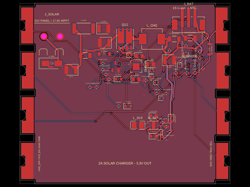 Similar packageShiboSoftwareDev/solar-battery-charger-moduleThis hardware setup integrates a solar panel, a lithium-ion battery, and a multi-rail buck converter with a battery charging IC, protection circuitry, and monitoring components, enabling solar power harvesting, battery charging, and power distribution in an embedded system.
 Discover something newimrishabh18/fitness_watchThis circuit integrates an ESP-12E microcontroller with various sensors and peripherals, including a AO3400A MOSFET for switching loads, to enable wireless control and sensor data processing.