imrishabh18/corne-keyboard
The code defines and renders two surface-mount chip components with SMT pads, silkscreen outlines, and 3D CAD models (OBJ and STEP) for PCB assembly.
- Version
- 2.0.21
- License
- unset
- Stars
- 1
scripts/audit-pour-clearance.py
"""Independent same-layer pour-to-other-net copper clearance audit.

Usage: python audit-pour-clearance.py circuit.json report.json [--required .2]
Requires Shapely. Reports all known-net and unassigned copper separately; it does
not change the circuit, suppress DRC, or treat net labels as geometric contacts.
"""
import argparse, json, math, hashlib
from collections import defaultdict
from pathlib import Path
from shapely.geometry import Point, Polygon, LineString, box
from shapely.affinity import rotate, translate
from shapely.strtree import STRtree
from shapely.ops import unary_union

p=argparse.ArgumentParser();p.add_argument('input');p.add_argument('output');p.add_argument('--required',type=float,default=.2);a=p.parse_args()
data=Path(a.input).read_bytes();j=json.loads(data)
parent={}
def root(x):
 parent.setdefault(x,x)
 if parent[x]!=x:parent[x]=root(parent[x])
 return parent[x]
def join(xs):
 xs=[x for x in xs if x]
 if not xs:return
 for x in xs[1:]:parent[root(x)]=root(xs[0])
def key(e):return 'key:'+e['subcircuit_connectivity_map_key'] if e.get('subcircuit_connectivity_map_key') else None
# Source-net equivalence includes explicit internal connections. PCB geometry
# never establishes logical equivalence, so touching other-net copper stays an error.
for e in j:
 t=e['type']
 if t=='source_trace':join([e['source_trace_id'],key(e),*e['connected_source_port_ids'],*e['connected_source_net_ids']])
 elif t=='source_net':join([e['source_net_id'],key(e)])
 elif t=='source_port':join([e['source_port_id'],key(e)])
 elif t=='source_component_internal_connection':join(e['source_port_ids'])
ports={e['pcb_port_id']:e for e in j if e['type']=='pcb_port'}
sports={e['source_port_id']:e for e in j if e['type']=='source_port'}
components={e['source_component_id']:e for e in j if e['type']=='source_component'}
traces={e['pcb_trace_id']:e for e in j if e['type']=='pcb_trace'}
boards=[e for e in j if e['type']=='pcb_board']
metadata_conflicts=[]
def net(e):
 candidates=[]
 if e.get('pcb_port_id') in ports:candidates.append(ports[e['pcb_port_id']].get('source_port_id'))
 candidates.extend([key(e),e.get('source_net_id'),e.get('source_trace_id')])
 if e.get('connection_name') in parent:candidates.append(e['connection_name'])
 if e['type']=='pcb_via' and e.get('pcb_trace_id') in traces:candidates.append(net(traces[e['pcb_trace_id']]))
 resolved={root(x) for x in candidates if x and x in parent}
 if len(resolved)>1:metadata_conflicts.append({'id':e.get(e['type']+'_id'),'nets':sorted(resolved)})
 return sorted(resolved)[0] if resolved else None
def label(e):
 pp=ports.get(e.get('pcb_port_id'));sp=sports.get(pp.get('source_port_id')) if pp else None
 return components.get(sp.get('source_component_id'),{}).get('name','?')+'.'+sp.get('name','?') if sp else e.get(e['type']+'_id')
def ring(r):
 if any(v.get('bulge') for v in r['vertices']):raise ValueError('Arc BRep ring not supported')
 return [(v['x'],v['y']) for v in r['vertices']]
def pill(w,h):
 r=min(w,h)/2
 if abs(w-h)<1e-9:return Point(0,0).buffer(r,quad_segs=128)
 return LineString([(-(w/2-r),-(h/2-r)),(w/2-r,h/2-r)]).buffer(r,quad_segs=128)
def rect(w,h,r=0):return box(-w/2+r,-h/2+r,w/2-r,h/2-r).buffer(r,quad_segs=64) if r else box(-w/2,-h/2,w/2,h/2)
def copper(e):
 t=e['type'];s=e.get('shape');rotation=e.get('ccw_rotation',0)
 if t=='pcb_copper_pour':
  if s=='brep':
   b=e['brep_shape'];g=Polygon(ring(b['outer_ring']),[ring(r) for r in b['inner_rings']])
  elif s=='polygon':g=Polygon([(p['x'],p['y']) for p in e['points']])
  elif s=='rect':g=translate(rotate(rect(e['width'],e['height']),e.get('rotation',0),origin=(0,0)),e['center']['x'],e['center']['y'])
  else:raise ValueError(s)
  if not g.is_valid:raise ValueError('Invalid copper pour')
  return g
 if t=='pcb_via':g=Point(0,0).buffer(e['outer_diameter']/2,quad_segs=128).difference(Point(0,0).buffer(e['hole_diameter']/2,quad_segs=128))
 elif t=='pcb_smtpad':
  if s=='polygon':return Polygon([(p['x'],p['y']) for p in e['points']])
  if s=='circle':g=Point(0,0).buffer(e['radius'],quad_segs=128)
  elif s in ['rect','rotated_rect']:g=rect(e['width'],e['height'],e.get('corner_radius',0))
  elif s in ['pill','rotated_pill']:g=pill(e['width'],e['height'])
  else:raise ValueError(s)
 elif t=='pcb_plated_hole':
  if s=='circle':g=Point(0,0).buffer(e['outer_diameter']/2,quad_segs=128);hole=Point(0,0).buffer(e['hole_diameter']/2,quad_segs=128)
  elif s=='pill':g=pill(e['outer_width'],e['outer_height']);hole=pill(e['hole_width'],e['hole_height'])
  elif s in ['circular_hole_with_rect_pad','pill_hole_with_rect_pad','rotated_pill_hole_with_rect_pad']:
   rotation=0;g=rotate(rect(e['rect_pad_width'],e['rect_pad_height'],e.get('rect_border_radius',0)),e.get('rect_ccw_rotation',0),origin=(0,0))
   hole=Point(0,0).buffer(e['hole_diameter']/2,quad_segs=128) if 'hole_diameter' in e else rotate(pill(e['hole_width'],e['hole_height']),e.get('hole_ccw_rotation',0),origin=(0,0))
   hole=translate(hole,e.get('hole_offset_x',0),e.get('hole_offset_y',0))
  else:raise ValueError(s)
  g=g.difference(hole)
 else:raise ValueError(t)
 return translate(rotate(g,rotation,origin=(0,0)),e['x'],e['y'])

nodes=[];pours=[]
for e in j:
 t=e['type']
 if t=='pcb_copper_pour':pours.append((e,copper(e),e['layer'],net(e)));continue
 if t in ['pcb_smtpad','pcb_plated_hole','pcb_via']:
  g=copper(e)
  for layer in e.get('layers',[e.get('layer')]):nodes.append((e,g,layer,net(e)))
 elif t=='pcb_trace':
  bylayer=defaultdict(list)
  for start,end in zip(e['route'],e['route'][1:]):
   if start['route_type']=='wire' and end['route_type']=='wire' and start['layer']==end['layer']:
    bylayer[start['layer']].append(LineString([(start['x'],start['y']),(end['x'],end['y'])]).buffer(min(start['width'],end['width'])/2,quad_segs=64))
  for layer,segments in bylayer.items():nodes.append((e,unary_union(segments),layer,net(e)))
# Compare pours to other pours too when designs contain multiple pour nets.
nodes.extend(pours)
violations=[];minima={};measured_pairs=0
for layer in sorted({x[2] for x in nodes}):
 ns=[n for n in nodes if n[2]==layer];tree=STRtree([n[1] for n in ns])
 for pe,pg,pl,pn in pours:
  if pl!=layer:continue
  board=min(boards,key=lambda b:pg.centroid.distance(Point(b['center']['x'],b['center']['y'])))['pcb_board_id']
  for k in tree.query(pg.buffer(a.required+.02)):
   e,g,l,n=ns[k]
   if e is pe or pn is not None and pn==n:continue
   measured_pairs+=1;d=pg.distance(g);kind='known_other_net' if n else 'unassigned_copper';group=board+':'+kind
   minima[group]=min(minima.get(group,math.inf),d)
   if d>=a.required-1e-5:continue
   inter=pg.intersection(g) if d<=1e-9 else None
   violations.append({'board':board,'pour_id':pe['pcb_copper_pour_id'],'copper_id':e[e['type']+'_id'],'copper_type':e['type'],'copper_shape':e.get('shape'),'label':label(e),'layer':layer,'net':n,'kind':kind,'clearance_mm':d,'contact':d<=1e-9,'contact_area_mm2':inter.area if inter is not None else 0,'contact_length_mm':inter.length if inter is not None else 0,'material_clearance_violation':d<a.required-.01})
summary={}
for board in [e['pcb_board_id'] for e in boards]:
 summary[board]={}
 for kind in ['known_other_net','unassigned_copper']:
  v=[x for x in violations if x['board']==board and x['kind']==kind]
  summary[board][kind]={'minimum_measured_clearance_mm':minima.get(board+':'+kind),'contacts':sum(x['contact'] for x in v),'below_required_by_over_0p01mm':sum(x['material_clearance_violation'] for x in v),'below_nominal_by_over_0p00001mm':len(v)}
report={'input':str(Path(a.input).resolve()),'input_sha256':hashlib.sha256(data).hexdigest(),'required_clearance_mm':a.required,'summary':summary,'metadata_conflicts':metadata_conflicts,'measured_candidate_pairs':measured_pairs,'violations':sorted(violations,key=lambda x:x['clearance_mm']),'limits':['Complements connectivity audit; does not establish intended-net connectivity or manufacturing readiness.','Net equivalence includes source traces, source net keys, and declared internal connections; unassigned mounting PTHs remain separate.','Uses BRep outlines and holes exactly for straight edges; arc bulges are rejected.','Round copper uses 512-segment circle approximations; routing segments use 256-segment round caps.','Solver output commonly approximates circular clearances with 32 sides, so measured .1966mm may represent a nominal .2mm clearance. Differences below .01mm are reported separately from larger violations, never silently called exact compliance.','Trace copper assumes same-layer wire segments and uses the smaller endpoint width; through vias and plated-hole pads are checked on all declared layers.','No solder-mask, thermal, annular ring, milling tolerance, or fabrication output checks.']}
Path(a.output).write_text(json.dumps(report,indent=2));print(json.dumps({'summary':summary,'metadata_conflicts':metadata_conflicts},indent=2))
Related Packages
 More from this authorimrishabh18/boost-converterThis code defines a PCB schematic and 3D model layout focusing on a power conversion circuit with components like USB-C connector, MT3608 step-up regulator, inductor, diode, input/output capacitors, and resistors arranged on a double-layer PCB.
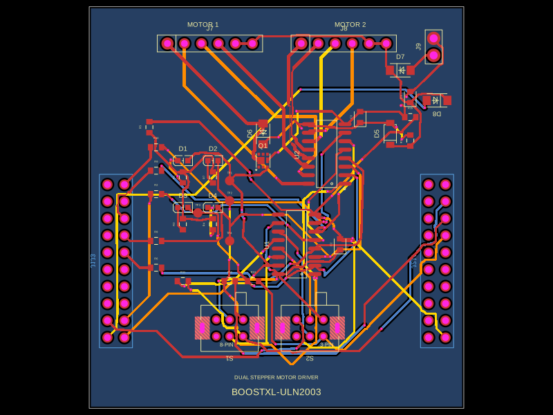 Similar packageabse/boostxl-uln2003This code defines a React component that models a through-hole or surface-mount LED with specified pin labels, footprint, silkscreen, and 3D CAD model for PCB layout.
 Discover something newhrithik18k/smart-switch-pcbThe AO3400A component models a SOT-23 N-channel MOSFET with labeled pins for Gate, Source, and Drain, including 3D CAD models and schematic symbols for electronic circuit design.