imrishabh18/corne-keyboard
The code defines and renders two surface-mount chip components with SMT pads, silkscreen outlines, and 3D CAD models (OBJ and STEP) for PCB assembly.
- Version
- 2.0.21
- License
- unset
- Stars
- 1
scripts/audit-copper.py
import json, sys, math
from collections import defaultdict
from shapely.geometry import Point, Polygon, LineString, box
from shapely.affinity import rotate, translate
from shapely.strtree import STRtree
from shapely.ops import unary_union

# Measure physical contacts. Net names only choose the intended copper; they
# never join geometrically separate pieces. BRep holes are preserved.
j=json.load(open(sys.argv[1]))
if len(sys.argv)>3:
 key=sys.argv[3]
 net=next((e for e in j if e['type']=='source_net' and e.get('subcircuit_connectivity_map_key')==key),{'source_net_id':'__unnamed__','subcircuit_connectivity_map_key':key})
else:
 net=next(e for e in j if e['type']=='source_net' and e['name']=='GND')
key=net['subcircuit_connectivity_map_key']
sourceports={p for e in j if e['type']=='source_trace' and e.get('subcircuit_connectivity_map_key')==key for p in e['connected_source_port_ids']}
ports={e['pcb_port_id']:e for e in j if e['type']=='pcb_port' and e.get('source_port_id') in sourceports}
sp={e['source_port_id']:e for e in j if e['type']=='source_port'}
sc={e['source_component_id']:e for e in j if e['type']=='source_component'}
def label(p):
 s=sp[p['source_port_id']]
 return sc[s['source_component_id']]['name']+'.'+s['name']
def ring(r):
 assert all(not v.get('bulge') for v in r['vertices'])
 return [(v['x'],v['y']) for v in r['vertices']]
def pill(w,h):
 r=min(w,h)/2
 if abs(w-h)<1e-9:return Point(0,0).buffer(r,quad_segs=64)
 return LineString([(-(w/2-r),-(h/2-r)),(w/2-r,h/2-r)]).buffer(r,quad_segs=64)
def rect(w,h,r=0):
 return box(-w/2+r,-h/2+r,w/2-r,h/2-r).buffer(r,quad_segs=32) if r else box(-w/2,-h/2,w/2,h/2)
def copper(e):
 t=e['type'];s=e.get('shape');a=e.get('ccw_rotation',0)
 if t=='pcb_copper_pour':
  b=e['brep_shape'];g=Polygon(ring(b['outer_ring']),[ring(r) for r in b['inner_rings']]);assert g.is_valid;return g
 if t=='pcb_via':g=Point(0,0).buffer(e['outer_diameter']/2,quad_segs=64).difference(Point(0,0).buffer(e['hole_diameter']/2,quad_segs=64))
 elif t=='pcb_smtpad':
  if s=='polygon':return Polygon([(p['x'],p['y']) for p in e['points']])
  if s=='circle':g=Point(0,0).buffer(e['radius'],quad_segs=64)
  elif s in ['rect','rotated_rect']:g=rect(e['width'],e['height'],e.get('corner_radius',0))
  elif s in ['pill','rotated_pill']:g=pill(e['width'],e['height'])
  else:raise ValueError(s)
 elif t=='pcb_plated_hole':
  if s=='circle':g=Point(0,0).buffer(e['outer_diameter']/2,quad_segs=64);h=Point(0,0).buffer(e['hole_diameter']/2,quad_segs=64)
  elif s=='pill':g=pill(e['outer_width'],e['outer_height']);h=pill(e['hole_width'],e['hole_height'])
  elif s in ['circular_hole_with_rect_pad','pill_hole_with_rect_pad','rotated_pill_hole_with_rect_pad']:
   a=0;g=rotate(rect(e['rect_pad_width'],e['rect_pad_height'],e.get('rect_border_radius',0)),e.get('rect_ccw_rotation',0),origin=(0,0))
   h=Point(0,0).buffer(e['hole_diameter']/2,quad_segs=64) if 'hole_diameter' in e else rotate(pill(e['hole_width'],e['hole_height']),e.get('hole_ccw_rotation',0),origin=(0,0))
   h=translate(h,e.get('hole_offset_x',0),e.get('hole_offset_y',0))
  else:raise ValueError(s)
  g=g.difference(h)
 else:raise ValueError(t)
 return translate(rotate(g,a,origin=(0,0)),e['x'],e['y'])

nodes=[];parent=[];bylayer=defaultdict(list);portnodes=defaultdict(list)
def root(i):
 while parent[i]!=i:parent[i]=parent[parent[i]];i=parent[i]
 return i
def join(a,b):parent[root(a)]=root(b)
def add(e,g,layer,id):
 i=len(nodes);nodes.append((e,g,layer,id));parent.append(i);bylayer[layer].append(i)
 if e.get('pcb_port_id') in ports:portnodes[e['pcb_port_id']].append(i)
 return i
ground_source_traces={e['source_trace_id'] for e in j if e['type']=='source_trace' and e.get('subcircuit_connectivity_map_key')==key}
traces={e['pcb_trace_id']:e for e in j if e['type']=='pcb_trace' and (e.get('subcircuit_connectivity_map_key')==key or e.get('source_net_id')==net['source_net_id'] or e.get('connection_name')==net['source_net_id'] or e.get('source_trace_id') in ground_source_traces)}
for e in j:
 t=e['type']
 if t in ['pcb_smtpad','pcb_plated_hole'] and e.get('pcb_port_id') in ports or t=='pcb_copper_pour' and e.get('source_net_id')==net['source_net_id'] or t=='pcb_via' and (e.get('subcircuit_connectivity_map_key')==key or e.get('source_net_id')==net['source_net_id'] or e.get('pcb_trace_id') in traces):
  g=copper(e);id=e[t+'_id'];ids=[add(e,g,l,id) for l in e.get('layers',[e.get('layer')])]
  if t in ['pcb_plated_hole','pcb_via']:
   for i in ids[1:]:join(ids[0],i)
 if t=='pcb_trace' and e['pcb_trace_id'] in traces:
  for a,b in zip(e['route'],e['route'][1:]):
   if a['route_type']=='wire' and b['route_type']=='wire' and a['layer']==b['layer']:
    g=LineString([(a['x'],a['y']),(b['x'],b['y'])]).buffer(min(a['width'],b['width'])/2,quad_segs=32)
    add(e,g,a['layer'],e['pcb_trace_id'])
for layer,ids in bylayer.items():
 tree=STRtree([nodes[i][1] for i in ids])
 for i in ids:
  g=nodes[i][1]
  for local in tree.query(g.buffer(1e-6)):
   k=ids[local]
   if k>i and g.distance(nodes[k][1])<=1e-6:join(i,k)
groups=defaultdict(list)
for pid,p in ports.items():
 ns=portnodes[pid];assert ns,('missing copper',pid)
 # Duplicate SMT shapes may share a port but are joined only by actual copper.
 rs={root(i) for i in ns};assert len(rs)==1,('split footprint pad',pid,rs)
 groups[next(iter(rs))].append({'id':pid,'name':label(p),'x':p['x'],'y':p['y']})
sortedgroups=sorted(groups.items(),key=lambda kv:-len(kv[1]))
report={'input':sys.argv[1],'connectivity_key':key,'ground_port_count':len(ports),'pour_island_count':sum(e['type']=='pcb_copper_pour' and e.get('source_net_id')==net['source_net_id'] for e in j),'physical_ground_groups':len(groups),'groups':[]}
for r,ps in sortedgroups:
 pours={nodes[i][3] for i in range(len(nodes)) if root(i)==r and nodes[i][0]['type']=='pcb_copper_pour'}
 report['groups'].append({'port_count':len(ps),'pour_ids':sorted(pours),'ports':ps})
report['floating_pour_islands']=sorted({nodes[i][3] for i in range(len(nodes)) if nodes[i][0]['type']=='pcb_copper_pour' and root(i) not in groups})
report['pour_connected_trace_endpoints']=[]
if len(groups)==1:
 connected_root=next(iter(groups))
 connected_pours=[(nodes[i][3],nodes[i][1],nodes[i][2]) for i in range(len(nodes)) if root(i)==connected_root and nodes[i][0]['type']=='pcb_copper_pour']
 for trace in traces.values():
  for end,p in [('start',trace['route'][0]),('end',trace['route'][-1])]:
   if p['route_type']!='wire':continue
   touched=[id for id,g,l in connected_pours if l==p['layer'] and g.covers(Point(p['x'],p['y']))]
   if touched:report['pour_connected_trace_endpoints'].append({'trace_id':trace['pcb_trace_id'],'end':end,'pour_ids':touched})
out=sys.argv[2];json.dump(report,open(out,'w'),indent=2)
print({k:v for k,v in report.items() if k not in ['groups','floating_pour_islands','pour_connected_trace_endpoints']})
print('Group sizes:',[g['port_count'] for g in report['groups']])
for g in report['groups']:print(g['port_count'],', '.join(p['name'] for p in g['ports']))
print('Floating pour islands:',len(report['floating_pour_islands']))
Related Packages
 More from this authorimrishabh18/boost-converterThis code defines a PCB schematic and 3D model layout focusing on a power conversion circuit with components like USB-C connector, MT3608 step-up regulator, inductor, diode, input/output capacitors, and resistors arranged on a double-layer PCB.
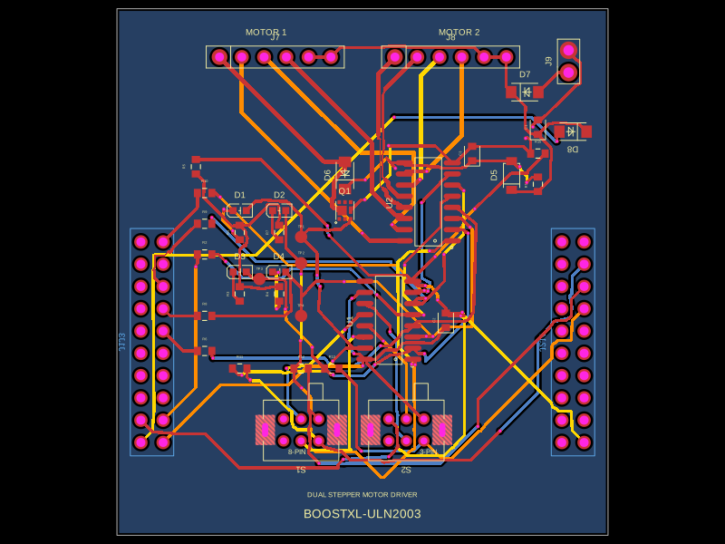 Similar packageabse/boostxl-uln2003This code defines a React component that models a through-hole or surface-mount LED with specified pin labels, footprint, silkscreen, and 3D CAD model for PCB layout.
 Discover something newhrithik18k/smart-switch-pcbThe AO3400A component models a SOT-23 N-channel MOSFET with labeled pins for Gate, Source, and Drain, including 3D CAD models and schematic symbols for electronic circuit design.