gokul/acoustic-guitar-tuner
This code defines the physical pin configuration and footprint layouts for the ATtiny1616 microcontroller and a matching tactile switch component, including their key hardware connection points, dimensions, and 3D models.
- Version
- 1.0.10
- License
- unset
- Stars
- 1
MANUFACTURING.md
# Manufacturing and validation status

**Engineering prototype v1.0.10 - production approval pending.** The CAD checks pass, but no physical prototype has been tested. Submit the new manufacturing/ files for manufacturer review before ordering a small first article. Do not treat software checks as proof of acoustic performance, assembly yield or battery life. Older test-pad archives have been preserved locally under .tscircuit/archive/ and are obsolete.

## Intended specification

- Custom guitar profile, maximum 40 x 70 mm; two layers, 1.6 mm FR-4, 1 oz copper.
- ENIG recommended for the fine-pitch QFN and small microphone lands.
- Via drill 0.3 mm, copper diameter 0.6 mm; board-edge clearance at least 0.3 mm.
- Top-side SMD parts and through-hole female J1; bottom-side CR2032 holder.
- J1 supplier C2897366, BOOMELE PM254-1-03-Z-8.5, pitch 2.54 mm, nominal finished holes 1.02 mm, housing height 8.5 mm. Confirm drill tolerance with the assembler.
- 2.8 mm NPTH mounting hole and approximately 0.5 mm NPTH microphone aperture.
- No charger or reverse-battery protection. Fit the cell only after assembly/programming.

## Assembly requirements

1. Verify exact parts and assembly orientation. LED physical pin 1 is cathode; pin 2 is anode.
2. Have the assembler approve QFN exposed-pad paste coverage and stencil design.
3. Keep MK1's bottom sound aperture open and aligned. Its four ground sectors are physical pin 3; extra software port numbers are modeling identifiers only.
4. Follow the microphone datasheet: no ultrasonic cleaning/board washing, no pressure/vacuum applied to the port, controlled reflow (260 C maximum, no more than three cycles).
5. Solder J1 and the bottom battery holder without blocking the aperture. Check connector tails/solder joints cannot touch the battery or enclosure. Verify holder polarity before fitting the cell, positive face outward.
6. Agree panel rails, support and optical fiducials with the assembler. The custom outline is not automatically suitable for a conveyor.

## Release gates

- [x] Type, netlist and PCB placement checks pass without actionable violations.
- [x] Every required net is routed; no routing, disconnected-port or edge-clearance errors.
- [x] Gerber-derived short-circuit checks pass on both layers.
- [x] CAD copper, drill, mask, silk and outline reviewed; assembler approval of paste and rotations still required.
- [x] Fresh BOM and placement files match this female-header revision.
- [ ] Manufacturer approves trace/space, annular rings, drill tolerance, stencil and panel.
- [ ] Assembled first article passes electrical, acoustic, battery and programming tests.

Only after CAD/export gates pass should a small engineering sample be fabricated. Production approval additionally requires physical tests; software-only checks cannot certify 100% readiness.

The software also emits advisory warnings. Unnamed trace warnings concern source readability; built-in reference-designator styling warnings have been visually checked against rendered text. J1 uses a custom box symbol for a physical female connector, so its J prefix triggers a chip-type naming advisory. SW1's unused throw (pin 3) is intentionally open; its metal shell is grounded. BT1 is a power source, not a device requiring an input supply. Schematic spacing/simplification suggestions do not indicate missing copper, but the automatic layout is not a hand-drafted schematic.

The 10 MHz / 2.6 V BOD combination follows the operating-frequency table and its BOD note in the [Microchip ATtiny1614/1616/1617 datasheet](https://ww1.microchip.com/downloads/aemDocuments/documents/MCU08/ProductDocuments/DataSheets/40001893B.pdf). A depleted coin cell may trigger reset; the circuit is not intended to maintain operation across the cell's entire discharge curve.

## Supplied files

The Gerber ZIP contains copper, masks, paste, silkscreen, outline, plated/NPTH drills, BOM and placement CSVs. Separate CSV copies, assembly SVG, schematic PDF, KiCad archive and the compiled firmware HEX are also included in manufacturing/. The HEX does not set MCU fuses. manifest.json records SHA-256 hashes for this revision's source and artifacts. Old STEP models were not carried forward because they show the previous test-pad revision.

KiCad export correction: the pinned CLI's raw ZIP omitted its referenced child schematic. The supplied archive instead contains a flat, complete single-page schematic generated from the same circuit data using scripts/prepare-flat-kicad.mjs, and is DEFLATE-compressed. No component coordinates or net connections were changed by flattening. Treat supplier 3D models as illustrations, not the authority for solder land dimensions.

## First-article test

1. With no battery, inspect polarity/bridges and check VCC-to-GND resistance. Apply current-limited 3.3 V through J1; check supply current and VREF near half supply.
2. Program through J1: 1 UPDI, 2 regulated 3.3 V, 3 GND. Use megaTinyCore 2.6.11, ATtiny1616, internal 10 MHz, enabled 2.6 V BOD, retaining UPDI. Confirm fuses/readback. Never attach powered programming equipment with the cell installed.
3. Verify TEST sequences all nine LEDs individually and POWER disconnects the cell.
4. Measure actual ADC sampling cadence, clipping/headroom and pitch update latency. Apply accurate tones for all six strings; calibrate SAMPLE_CLOCK_SCALE.
5. Check sharp/flat/in-tune behavior, noise and octave rejection using an actual acoustic guitar at the intended distance.
6. Test temperature and loaded battery-voltage range. Internal oscillator drift and CR2032 voltage sag can affect accuracy; do not claim +/-4 cents or battery life without measurements.
7. Check microphone opening, connector access, battery replacement and mounting stress in the intended enclosure/clip.
Related Packages
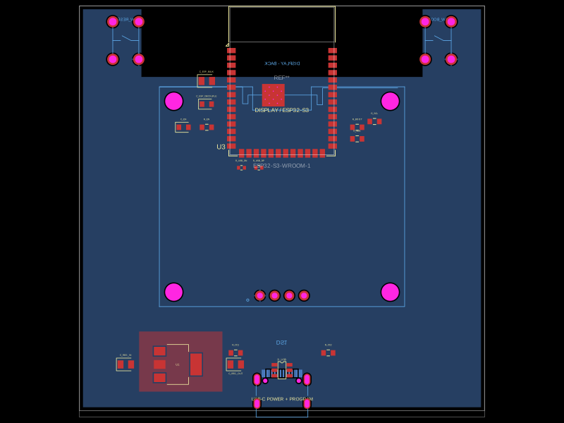 More from this authorgokul/board-v2This design integrates an ESP32-S3 Wi-Fi and Bluetooth module, a USB-C port with power and data circuitry, a USB ESD protection chip, a 3.3V voltage regulator, and an OLED display module on a PCB with associated routing and thermal copper pour layers.
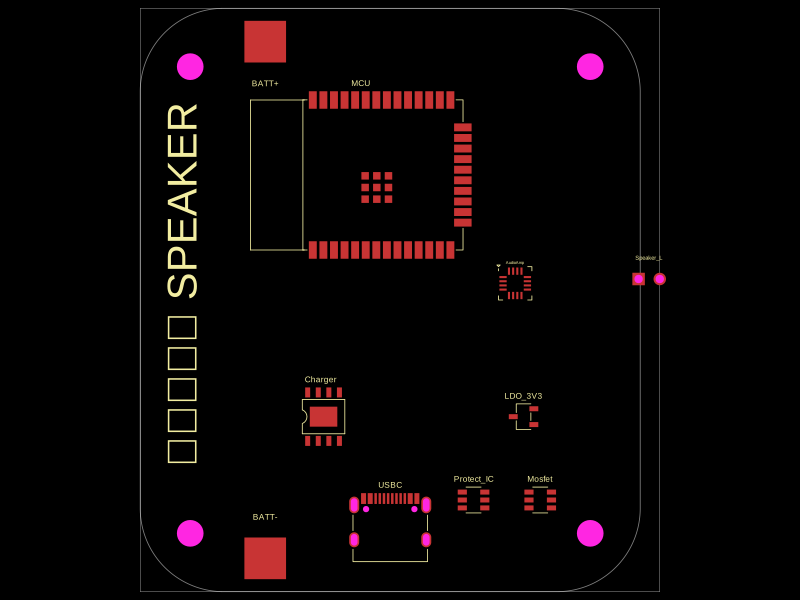 Similar packagemohan-bee/speakerThis code defines configurable 3D models and PCB footprints for various electronic components, including a battery charger IC, a dual Hall sensor, a dual power switch, and a voltage regulator, with detailed pinouts, footprints, and CAD models for schematic and physical design.
 Discover something newrushabhcodes/ESP32-E-ReaderThis code defines the physical layout and schematic wiring of an ESP32-based e-reader device, including various surface-mount components such as connectors, ICs, resistors, capacitors, inductors, diodes, pushbuttons, and an antenna, with precise PCB placement and interconnection details.